
Metallurgy Division Publications - NISTIR 7248
Technical Highlights |
MSEL Program OverviewsAdvanced Manufacturing Processes
NanometrologyNIST Contact: Debra L. Kaiser (Ceramics Division)Nanotechnology will revolutionize and possibly revitalize many industries, leading to new and improved products based on materials having at least one dimension less than 100 nm. The federal government's role in realizing the full potential of nanotechnology is coordinated through the National Nanotechnology Initiative (NNI), a multi-agency, multi-disciplinary program that supports research and development, invests in a balanced infrastructure, and promotes education, knowledge diffusion, and commercialization in all aspects of nanoscale science, engineering, and technology. NIST's unique and critical contribution to the NNI is nanometrology, defined as the science of measurement and/or a system of measures for nanoscale structures and systems. NIST nanometrology efforts focus on developing the measurement infrastructure - measurements, data, and standards - essential to advancing nanotechnology commercialization. This work provides the requisite metrology tools and techniques and transfers enabling measurement capabilities to the appropriate communities. MSEL plays a vital role in nanometrology work at NIST with efforts in four of the seven NNI Program Component Areas - Instrumentation Research, Metrology and Standards for Nanotechnology; Nanomaterials; Nanomanufacturing; and Fundamental Nanoscale Phenomena and Processes. Innovative projects across MSEL are defining and addressing the forefront research issues in these areas. Instrumentation Research, Metrology and Standards for NanotechnologyR&D pertaining to the tools needed to advance nanotechnology research and commercialization. The design, development, and fabrication of nanodevices will require nanomechanical measurements that are rapid, accurate, predictive, well-understood and representative of a device or system's environment in real time. MSEL is addressing this need by developing instrumentation, methodology, reference specimens and multi-scale modeling approaches to quantitatively measure mechanical properties such as modulus, strength, adhesion, and friction at nanometer-length scales. This year, novel instruments for measuring adhesion and friction forces between surfaces and nanoparticles were developed jointly with industrial partners. Quantitative maps of elastic modulus were obtained by innovative methodologies based on atomic force microscopy and strain-induced elastic buckling instability. To address the need for quantifying measurements made with widely-used commercial nanoindentors and scanned probe microscopy instruments, MSEL is developing reference specimens and SI-traceable force calibration methodology. NanomaterialsResearch aimed at discovery of novel nanoscale and nanostructured materials and at a comprehensive understanding of the properties of nanomaterials. Among the many classes of nanomaterials, nanotubes have received great attention due to their remarkable physical properties relevant to many applications. In response to needs expressed by industry and other federal agencies, MSEL has embarked on a new effort to develop a suite of metrologies and standards aimed at characterizing key structural features and processing variables of carbon nanotubes. These include dispersion, fractionation, orientation, alignment, and manipulation of individual single-walled nanotubes, all critical to establishing efficient bulk processing schemes to meet the imminent high demand for carbon nanotubes. NanomanufacturingR&D aimed at enabling scaled-up, reliable, cost-effective manufacture of nanoscale materials, structures, devices, and systems. Nanoimprint lithography (NIL) is rapidly emerging as a viable high-throughput technique for producing robust structures with a patterning resolution better than 10 nm. MSEL is developing metrologies that are crucial to advancing NIL as an industrial patterning technology for the electronics, optics, and biotechnology industries. The current focus is on characterizing shape and the fidelity of pattern transfer, two key factors in achieving widespread commercial application of NIL. Fundamental Nanoscale Phenomena and ProcessesDiscovery and development of fundamental knowledge pertaining to new phenomena in the physical, biological, and engineering sciences that occur at the nanoscale. The magnetic data storage industry needs the ability to measure and control magnetization on nanometer length scales and nanosecond time scales to meet increasing demands for reduced size and increased speed of devices. MSEL is developing measurement techniques to elucidate the fundamental mechanisms of spin dynamics and damping in magnetic thin films. Work this year has focused on measurements of the effects of interfaces and interface roughness on magnetization dynamics and magnetic characterization of edges in magnetic devices. Through these and other research activities, MSEL is maintaining its committed leadership in developing the measurement infrastructure for current and future nanotechnology-based applications. Back to Top
Materials for ElectronicsNIST Contact: Martin L. Green (Ceramics Division), Eric K. Lin (Polymers Division)The U.S. electronics industry faces strong international competition in the manufacture of smaller, faster, more functional, and more reliable products. Many critical challenges facing the industry require the continual development of advanced materials and processes. The NIST Materials Science and Engineering Laboratory (MSEL) works closely with U.S. industry, covering a broad spectrum of sectors including semiconductor manufacturing, device components, packaging, data storage, and assembly, as well as complementary and emerging areas such as optoelectronics and organic electronics. MSEL has a multidivisional approach, committed to addressing the most critical materials measurement and standards issues for electronic materials. Our vision is to be the key resource within the Federal Government for materials metrology development and will be realized through the following objectives:
The NIST/MSEL program consists of projects led by the Metallurgy, Polymers, Materials Reliability, and Ceramics Divisions. These projects are conducted in collaboration with partners from industrial consortia (e.g., SEMATECH), individual companies, academia, and other government agencies. The program is strongly coupled with other microelectronics programs within the government such as the National Semiconductor Metrology Program (NSMP). Materials metrology needs are also identified through the International Technology Roadmap for Semiconductors (ITRS), the International Packaging Consortium (IPC) Roadmap, the IPC Lead-free Solder Roadmap, the National Electronics Manufacturing Initiative (NEMI) Roadmap, the Optoelectronics Industry Development Association (OIDA) Roadmap, and the National Magnetic Data Storage Industry Consortium (NSIC) Roadmap. MSEL researchers from each division have made substantial contributions to the most pressing technical challenges facing industry, from new fabrication methods and advanced materials in the semiconductor industry, to low-cost organic electronics, and to novel classes of electronic ceramics. Below are just a few examples of MSEL contributions over the past year. Advanced Gate DielectricsTo enable further device scaling, the capacitive equivalent thickness (CET) of the gate stack thickness must be 0.5 nm to 1.0 nm. This is not achievable with existing SiO2/polcrystalline Si gate stacks. High dielectric constant gate insulators are needed to replace SiO2, and metal gate electrodes are needed to replace polycrystalline Si. Given the large number of possible materials choices for the gate dielectric/substrate and gate dielectric/metal gate electrode interfaces, the MSEL Ceramics Division is establishing a dedicated combinatorial film deposition facility to study the complex interfacial interactions. This same methodology is applicable to a wide variety of problems in the electronic materials field. Advanced LithographyLithography is the key enabling technology for the fabrication of advanced integrated circuits. As feature sizes decrease to sub-65 nm length scales, challenges arise because the image resolution and the thickness of the imaging layer approach the dimensions of the polymers used in the photoresist film. Unique high-spatial resolution measurements are developed to identify the limits of materials and processes for the development of photoresists for next-generation lithography. Advanced MetallizationAs the dimensions of copper metallization interconnects on microelectronic chips decrease below 100 nm, control of electrical resistivity becomes critical. The MSEL Metallurgy Division is developing seedless deposition methods that will simplify thin-film processing and result in film growth modes that increase trench filling, thus lowering interconnect resistivity. Mechanical Reliability of MicrochipsOne of the important ITRS challenges is to achieve effective control of the failure mechanisms affecting chip reliability. Detection and characterization methods for dimensionally constrained materials will be critical to the attainment of this objective. Scientists in the MSEL Materials Reliability Division are addressing this issue by focusing on electrical methods capable of determining the thermal fatigue lifetime and mechanical strength of patterned metal film interconnects essential to microchips. Back to Top
Advanced Manufacturing ProcessesNIST Contact: Frank W. Gayle (Metallurgy Division)The competitiveness of U.S. manufacturers depends substantially on their ability to create new product concepts and to quickly translate such concepts into manufactured products that meet their customers' increasing expectations of performance, cost, and reliability. This is equally true for well-established "commodity" industries, such as automotive, aerospace, and electronics; for materials suppliers of aluminum, steel, and polymers; and for rapidly growing industries based on nanotechnology and biotechnology. In support of these industries, MSEL is developing robust measurement methods, standards, software, and process and materials data needed for design, monitoring, and control of new and existing materials and their manufacturing processes. The Advanced Manufacturing Processes Program focuses on the following high-impact areas:
Our research is conducted in close collaboration with industrial partners, including industrial consortia, and with national standards organizations. These collaborations not only ensure the relevance of our research, but also promote rapid transfer and utilization of our research by our partners. Three projects from the Advanced Manufacturing Methods Program are highlighted below. NIST Combinatorial Methods Center (NCMC)The NCMC develops innovative combinatorial and high-throughput (C&HT) measurement techniques and experimental strategies for accelerating the discovery and optimization of complex materials and products, such as polymer coatings and films, structural plastics, fuels, personal care goods, and adhesives. These C&HT array and gradient methods enable the rapid acquisition and analysis of physical and chemical data from materials libraries, thereby accelerating materials discovery, manufacturing design, and knowledge generation. In 2005, the NCMC Consortium consisted of 19 institutions from industry, government laboratories, and academic groups, which represents a broad cross-section of the chemical and materials research sectors. A growing component of the NIST NCMC program is focused on accelerating the development and understanding of emerging technologies, including nanostructured materials, organic electronics, and biomaterials, and, in particular, on the nanometrology needed for C&HT-based research for these technologies. Forming of Lightweight MaterialsAutomotive manufacturing is a materials intensive industry that involves approximately 10 % of the U.S. workforce. In spite of the use of the most advanced, cost-effective technologies, this globally competitive industry has major productivity issues related to materials measurements, materials modeling, and process design. Chief among these is the difficulty of designing stamping dies for sheet metal forming. An ATP-sponsored workshop ("The Road Ahead," June 20-22, 2000) identified problems in the production of working die sets as the main obstacle to reducing the time between accepting a new design and actual production of parts. This is also the largest single cost (besides labor) in car production. Existing finite element models of deformation and the materials measurements and data on which they are based are inadequate to the task of evaluating a die set design: they do not accurately predict the multi-axial hardening, springback, and friction of sheet metal during metal forming processes and, therefore, the stamping dies designed using finite element analyses must be modified through physical prototyping to produce the desired shapes, particularly for high-strength steels and aluminum alloys. To realize the weight savings and increased fuel economy enabled by high-strength steel and aluminum alloys, a whole new level of formability measurement methods, models, and data is needed for accurate die design, backed by a better understanding of the physics behind metal deformation. The MSEL Metallurgy Division is working with the U.S. automakers and their suppliers to fill these needs. A key component of our program is the unique multi-axial deformation measurement facility with which local strains in deformed metal sheet can be measured in situ. This facility has enabled NIST to take a key role in developing new methods for assessing springback, residual stresses, friction between the sheet metal and die during forming, and surface roughening, and in providing benchmark data for international round-robin experiments for finite element code. New techniques for detecting local deformation events at surfaces are providing insights into the physics of deformation and are leading to physics-based constitutive equations. Hardness Standardization: Rockwell, Vickers, and KnoopHardness is the primary test measurement used to determine and specify the mechanical properties of metal products and, as such, determines compliance with customer specifications in the national and international marketplace. The MSEL Metallurgy Division is engaged in developing and maintaining national traceability for hardness measurements and in assisting U.S. industry in making measurements compatible with other countries around the world, enabled through our chairing the ASTM International Committee on Indentation Hardness Testing and heading the U.S. delegation to the ISO Committee on Hardness Testing of Metals, which oversees the development of the organizations' respective hardness programs. Our specific R&D responsibilities include the standardization of the national hardness scales, development of primary reference transfer standards, leadership in national and international standards writing organizations, and interactions and comparisons with U.S. laboratories and the National Metrology Institutes of other countries. Back to Top
Safety and ReliabilityNIST Contact: Thomas A. Siewert (Materials Reliability Division), Frank W. Gayle (Metallurgy Division)We take for granted that the physical infrastructure around us will perform day in and day out with consistent reliability. Yet, failures occur when these structures degrade to where they no longer sustain their design loads, or when they experience loads outside their original design considerations. In addition, we have become increasingly aware of our vulnerability to intentional attacks. The Safety and Reliability Program within MSEL was created to develop measurement technology to clarify the behavior of materials under extreme and unexpected loadings, to assess integrity and remaining life, and to disseminate guidance and tools to assess and reduce future vulnerabilities. Project selection is guided by identification and assessment of the particular vulnerabilities within our materials-based infrastructure, and focusing on those issues that would benefit strongly by improved measurements, standards, and materials data. This year, we have worked with the Department of Homeland Security and the Office of Science and Technology Policy in developing the National Critical Infrastructure R& D Plan, which will provide guidance across much of the national infrastructure. Ultimately, our goal is to moderate the effects of acts of terrorism, natural disasters, or other emergencies, all through improved use of materials. Our vision is to be the key resource within the Federal Government for materials metrology development as realized through the following objectives:
This program responds both to customer requests (primarily other government agencies) and to the Department of Commerce 2005 Strategic Goal of "providing the information and framework to enable the economy to operate efficiently and equitably." For example, engineering design can produce safe and reliable structures only when the property data for the materials are available and accurate. Equally important, manufacturers and their suppliers need to agree on how material properties should be measured. The Safety and Reliability Program works toward solutions to measurement problems on scales ranging from the macro to the micro. The scope of activities includes the development and innovative use of state-of-the-art measurement systems; leadership in the development of standardized test procedures and traceability protocols; development of an understanding of materials in novel conditions; and development and certification of Standard Reference Materials � (SRMs). Many of the tests involve extreme conditions, such as high rates of loading, high temperatures, or unusual environments (e.g., deep underwater). These extreme conditions often produce physical and mechanical properties that differ significantly from handbook values for their bulk properties under traditional conditions. These objectives will be realized through innovative materials property measurement and modeling.
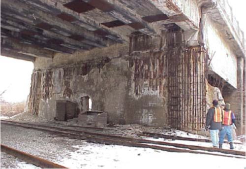
The MSEL Safety and Reliability Program is also contributing to the development of test method standards through committee leadership roles in standards development organizations such as the ASTM International and the International Standards Organization (ISO). In many cases, industry also depends on measurements that can be traced to NIST SRMs. In addition to the activities above, MSEL provides assistance to various government agencies on homeland security and infrastructural issues. Projects include assessing the performance of structural steels as part of the NIST World Trade Center Investigation, collaborating with both the Department of Transportation and the Department of Energy on pipeline safety and bridge integrity issues, advising the Bureau of Reclamation on metallurgical issues involving pipelines and dams, and advising the Department of the Interior on the structural integrity of the U.S.S. Arizona Memorial. Back to Top
|
|
|
|
Metallurgy Division of MSEL | metallurgy@nist.gov Home | Personnel | Research Opportunities The National Institute of Standards and Technology (NIST) is an agency of the U.S. Commerce Department. Privacy policy / security notice / accessibility statement / Disclaimer / Freedom of Information Act (FOIA) / No Fear Act Policy / ExpectMore.gov (performance of federal programs) / NIST Information Quality Standards |
Last modified: by Metallurgy Webmeister