
Metallurgy Division Publications - NISTIR 7248
Technical Highlights |

Nanometrology in the Metallurgy DivisionUltra-Low-Field Magnetic Sensors Antisymmetric Magnetoresistance Nanostructure Fabrication Processes
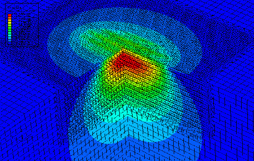
Nanomechanics: Atomistics in Modeling and ExperimentsNanoscale mechanical behavior (including failure) is inherently difficult to measure accurately, and existing modeling tools are only qualitative at best. We are developing modeling techniques that provide quantitative predictions and validating these results experimentally. NIST Contact: Lyle E. Levine, Douglas T. Smith, and Anne M. ChakaMechanics at the nanoscale is inherently difficult to model accurately. Finite element models (FEM) can effectively capture the elastic behavior of macroscopic structures but include no accurate failure criteria, since this depends upon atomic-scale behavior. Classical atomistic simulations can handle millions to billions of atoms, enough to model such events, but these potentials become inaccurate for large strains and cannot effectively handle chemistry. Quantum-mechanics-based simulations using density functional theory (DFT) are extremely accurate and handle the chemistry exactly, but such simulations are so CPU-intensive that they can handle only a few hundred atoms. A combination of all three modeling techniques is required to accurately model device behavior at the nanoscale. Over the past year, we have been developing quantitative multiscale modeling techniques for quasistatic applications. At the macroscale, FEM is used to simulate the elastic behavior of a nanomechanical system. Figure 1 shows an example in which a <111> Al crystal is indented by a nanoindenter. The shape of the nanoindenter was obtained using an atomic force microscope with closed-loop displacement control. The fine central mesh has nodes on fcc atom positions. The figure shows the resulting von Mises stress distribution (in cross-section) after indenting 1.5 nm.
Figure 1: FEM model of a rigid nanoindenter indenting a <111> aluminum single crystal to a depth of 1.5 nm. The use of classical potentials in a large simulation cell allows us to propagate long-range stresses to the critical regions where bond distortions are large or where chemistry effects need to be explored. In these critical regions, we embed a DFT simulation. The critical region is relaxed iteratively using DFT, and the classical cell is relaxed using a molecular dynamics algorithm.
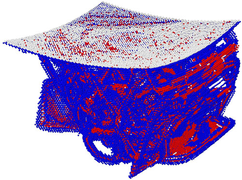
Figure 2: EAM simulation showing dislocations produced by nanoindentation of <111> Al to a depth of 4.5 nm. Figure 2 shows a classical atomistic simulation using the embedded atom method (EAM). Initial atom positions and boundary conditions came from a FEM simulation. The subsurface structure is composed of dislocations that nucleated from a single event. After an initial dislocation nucleation event, nanoindentation progresses through the complex evolution of dislocation structures. For example, the raised lip around an indent is produced by large numbers of dislocations exiting the surface. We are modeling the early stages of this process using 3D dislocation dynamics, assuming a random distribution of dislocation sources. Finally, connection to experimental measurements requires careful force calibration of the indenter and calibrated atomic force microscopy measurements of the indenter tip. We are setting up to grow bulk single-crystal copper samples, which will be cut and polished using non-contact chemical methods to minimize the dislocation density. We are also developing SI-traceable calibration methodology for nanoindenters and atomic force microscopes.
Contributors and CollaboratorsS.M. Khan, L. Ma, F. Tavazza, F. Biancaniello (Metallurgy Division, NIST); H. Burdette, B. Hockey, R. Wagner (Ceramics Division, NIST) Back to Top
NanomagnetodynamicsIn order to pursue the rapid development path set out for hard drives and magnetic memory, industry needs the ability to measure and control magnetization on nanometer length scales and nanosecond time scales. This project focuses on the metrology of spin dynamics and damping in magnetic thin films, especially on the properties of lithographically prepared edges of magnetic films. NIST Contact: Robert D. McMichaelWe develop measurement techniques to determine the static and dynamic properties of both continuous and patterned thin films of technologically important ferromagnetic metals and their interfaces with normal metals. The primary results this year include measurements of the affects of interfaces and interface roughness on magnetization dynamics and proof-of-concept experiments for measurements of lithographically prepared magnetic edges. These results have been communicated to the magnetic data storage industry through conference presentations, journal articles, and site visits.
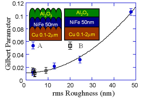
Figure 1: Damping as a function of roughness in Permalloy films on thick Cu substrates. The quadratic behavior is explained by a model featuring eddy currents that are excited by the roughness-induced stray magnetic fields in the copper. It is well known that surface affects and interfacial affects are important in nanostuctured materials. This is especially true for magnetic materials, where long-range interactions couple the surface magnetism to the bulk. Figure 1 shows a set of measurement results that show how interfacial properties affect damping in Ni80Fe20, (Permalloy) on a copper substrate. The increased damping is due to the excitation of eddy currents by magnetostatic fields associated with the roughness. We have also measured an additional component of interfacial damping that exists for smooth interfaces. We have started a new effort within this project to develop measurement techniques for characterization of magnetic edges. The edge properties of a magnetic device are critical because they affect the shape anisotropy of a patterned device and the nucleation of vortices in the critical stage for switching. While accepted techniques exist for characterizing bulk materials and interfaces, there are no such techniques available for characterizing the edges of thin film devices.
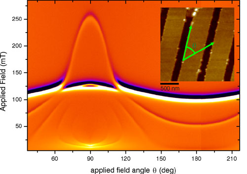
Figure 2: Image composed of 180 FMR spectra measured on an array of Permalloy stripes. An AFM image of the stripes is shown in the inset. At 90 ° the applied field is perpendicular to the stripes, and the peak is the resonance of the edge modes. Although the edge metrology aspect of the project has just started, we have already performed proof-of-concept magnetometry of edge saturation fields and ferromagnetic resonance measurements of localized edge modes (see Figure 2). These measurements are interpreted through corresponding micromagnetic modeling of the static and dynamic behavior of spins near edges. The stage is also set for magnetoresistive measurements that would be more suitable for wafer-level probing of the lithography process. Contributors and CollaboratorsJ. Rantschler, B. Maranville, J. Mallett, T. Moffatt, W. Egelhoff, Jr., A. Chen (Metallurgy Division, NIST); C. Ross, J. Cheng (MIT) Back to Top
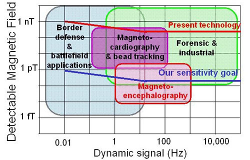
Materials for Ultra-Low-Field Magnetic SensorsMagnetic sensors play a central role in many important technologies ranging from health care to homeland security. A common need among these technologies is greater sensitivity and smaller size. A NIST competence program initiated in 2004 is focusing on developing the metrology that will enable new generations of magnetic sensors to be produced. NIST Contact: William F. Egelhoff, Jr.In the past decade, small inexpensive magnetic sensors have gained important footholds in a wide variety of technologies. Sales of small inexpensive magnetic sensors have been soaring. However, one relatively neglected aspect of these magnetic sensors has been their sensitivity to very small magnetic fields.
Figure 1: A plot of the sensitivity to very small magnetic fields that is required for various applications as a function of the frequency of the signal to be detected. Also indicated are the limits of present technology for small inexpensive solid-state sensors and the goals of the Competence Program. Figure 1 indicates, for particular applications, therange of fields that the sensor must be able to detect and the range of frequencies at which the fields appear. For comparison, the Earth's magnetic field is about 104 times larger than the top value of Figure 1. The plots of "Present technology" and "Our sensitivity goal" in Figure 1 indicate that deep inroads can potentially be made into important technologies if we can reach our goal. It should be pointed out that the technique of superconducting quantum interference devices (SQUIDs) can already reach sensitivities corresponding to the bottom values of Figure 1. Unfortunately, SQUIDs are expensive, bulky, and require cryogenic cooling. These factors rule out SQUIDs for all applications except those for which size and cost are not a factor and for which cryogenic cooling is not prohibitively inconvenient. We are focusing on small inexpensive thin-film magnetic sensors to avoid the disadvantages of SQUIDs. Existing precedents suggest that such sensors could be mass produced at a cost of a few cents each, will have a size measured in microns, and will operate at room temperature. These characteristics make them ideal for the applications indicated in Figure 1. To achieve our goal we will need magnetic thin films of great sensitivity. The best thin films previously known had susceptibilities of a few thousand. In our first year of work, we have already achieved values above 100 thousand. One of the prime applications that we may impact is magneto-cardiography, or imaging the beating heart in real time. In principle, magneto-cardiography could give very high quality 3-D images. However, at present, SQUID-based magneto-cardiography is hugely expensive, has poor resolution, and is practiced only at a few research institutions. If small, inexpensive sensors could make high-resolution magneto-cardiography generally available, it would change the practice of cardiology. The following quote arose in a discussion of our plans. "Real-time magneto-cardiography with 1 cm resolution would have revolutionary diagnostic impact."Bob Balaban, As Figure 1 would suggest, magneto-encephalography may be too demanding an application for the magnetic sensors we envision. However, it is always difficult to forecast the limits on new technologies. The one thing that is very clear is that we have very little competition in this field of research. The companies that currently produce the small, inexpensive magnetic sensors do not have active research and development programs in the area of ultra-low fields. The narrow profit margins for existing products will not support such programs. This situation puts NIST in an ideal position to take the lead and perform a high-risk/high-payoff research program that would not otherwise be undertaken. Contributors and CollaboratorsR. McMichael, C. Dennis, F. Johnson, B. Maranville, J. Rantschler, A. Shapiro (Metallurgy Division, NIST); J. Unguris (Physics Lab, NIST); D. Pappas, S. Russek(EEEL, NIST) Back to Top
A New Type of Antisymmetric Magnetoresistance in Materials with Perpendicular AnisotropyWhen the magnetization reverses direction in a ferro-magnet upon the application of a reversed magnetic field, it usually occurs by the nucleation of local domains with a reversed magnetization vector which subsequently grows to envelop the whole material. The ease (or difficulty) by which such a process occurs is key to determining how useful that material will be for its intended application. The metrology for detecting, measuring, and imaging the process in various classes of materials is being developed in this project. This knowledge is necessary for quick implementation of new magnetic materials for the recording, refrigeration, theft control, and power industries. NIST Contact: Robert D. Shull, Valerian I. Nikitenko, and Alexander J. ShapiroThe simplest way to detect the magnetic state of a material is to sense the magnetic field that surrounds it. However, as magnetic devices are reduced in size, the magnitude and spatial extent of these fields are also reduced. Recently, very sensitive field sensors (e.g., giant (GMR), tunneling (TMR), and colossal (CMR) magnetoresistance detectors) have been developed which are based upon measuring the resistance changes caused by the presence of small magnetic fields. In all these devices, the resistance changes are all symmetric with respect to the sign of the magnetic field. We report here the discovery of a new magnetoresistance effect in a multilayer which changes sign with changes in the direction of the magnetic field. Furthermore, the phenomenon is found to be caused by the presence of domain walls running perpendicular to the current direction.
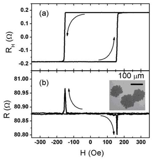
Figure 1: Arrows denote the sequence of measurements; inset shows the domain patterns correlated with magnetization reversal at the MR and RH peaks. Figure 1 shows the antisymmetric Hall resistance (RH) and in-line resistance (R) for a [Co(0.6 nm)/ Pt(1 nm)]4 multilayer as the magnetic field (H) is cycled between positive and negative fields. Note that ΔR(H) = -ΔR(-H) in (b), indicating the magnetoresistance (MR) is negative when switching from negative fields to positive fields while it is positive when switching from positive fields to negative fields, is similar to the Hall effect but quite different from normal MR phenomena.
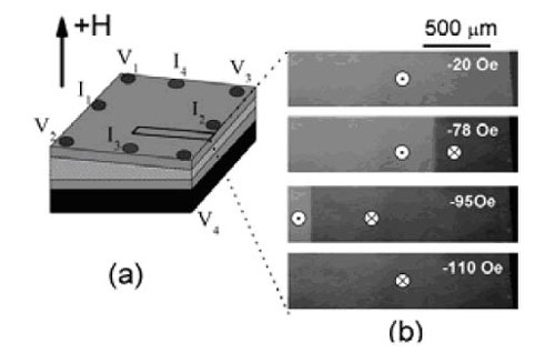
Figure 2: Wedge sample showing: (a) leads for measuring current, I, and voltage, V; (b) domain positions as a function of field. By the controlled creation of a single domain wall running perpendicular to the current direction (shown in Figure 2), the antisymmetric magnetoresistance has been shown to be due to the presence of such a domain wall. This configuration was created by preparing a trilayer containing a wedge-shaped Co layer (varying in thickness from 0.3 nm to 0.6 nm) sandwiched by 3 nm thick Pt layers. We had earlier found in such a trilayer that one could create such a single domain wall running perpendicular to the wedge at a position along the wedge determined by the magnitude of the reversed field applied, as shown in Figure 2(b). The unusual magnetoresistance effect is due to circulating currents created at the domain wall due to the opposite Hall voltages on either side of the wall. The results, which were published in Phys. Rev. Letters 94, 17203 (2005), provide much more flexibility to the circuit designers and may point the way to creating double pole magnetic switches. Contributors and CollaboratorsX. Cheng, S. Urazhdin, O. Tchernyshyov, C. Chien (Johns Hopkins University) Back to Top
Nanostructure Fabrication Processes: Surface & Growth Stress During Thin Film ElectrodepositionThe adsorption of species onto a surface alters the surface stress since the local interaction of each adsorbate alters the bond strength between neighboring atoms on the surface. Our immediate focus is to use surface stress to examine substrate-adsorbate interactions of various molecules for self-assembled monolayers (SAM). A natural extension of this work is to examine the surface stress associated with adsorbate-adsorbate lateral interactions. This could lead to a general in situ metrology for control of surfactants and adsorbate-based surface modification for a variety of molecular electronics and sensor applications. NIST Contact: Gery R. Stafford and Carlos BeauchampSurface stresses arise because the atomic configuration of atoms at a surface is different from the bulk. Interior atoms exert a stress on the surface atoms, i.e., the surface stress, which moves them out of the positions they would occupy in a bulk crystal configuration. The adsorption of species onto the surface can be expected to alter the surface stress since the local interaction of each adsorbate will alter the bond strength between neighboring atoms on the surface. An understanding of adsorbate-induced surface stress is critical to emerging technologies such as molecular electronics, nanostructure fabrication, and chemical/biological sensors. We have established a Class II (1 mW) HeNe optical bench dedicated to in situ measurement of surface and growth stress during electrochemical processing using the wafer curvature method. Measurements are made on a borosilicate glass cantilever onto which 250 nm of Au is evaporated. The curvature of the substrate is monitored while in solution and under potential control by reflecting a HeNe laser off the glass/metal interface, through a series of mirrors, and onto a position-sensitive detector. The relationship between force exerted onto the cantilever by the electrochemical processes occurring at the Au-solution interface and the radius of curvature of the cantilever is given by Stoney's equation. Forces on the order of 0.008 N/m (23 km radius of curvature) can be resolved. This is sufficient to study the adsorption of molecular monolayers onto the electrode surface. As a demonstration, we have measured the surface stress associated with reversible monolayer adsorption of both sulfate and chloride ions onto the Au surface from aqueous solutions.
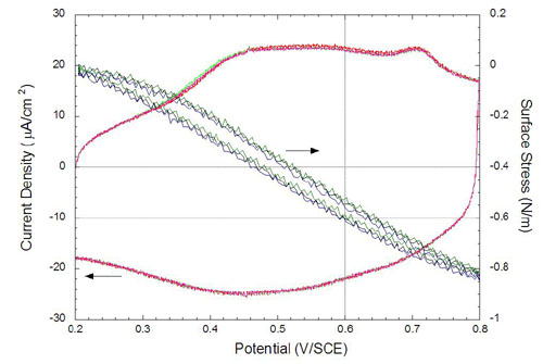
Figure 1: Linear sweep voltammetry and surface stress associated with sulfate adsorption on (111)-textured Au in 1.0 mol/L H2SO4.
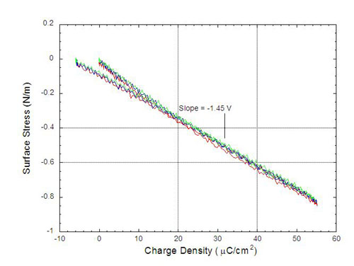
Figure 2: Surface stress vs. charge density associated with sulfate adsorption on (111)-textured Au in 1.0 mol/L H2SO4. Figure 1 shows the linear sweep voltammetry (three consecutive transients taken 5 minutes apart) as well as the associated surface stress of a (111)-textured Au electrode in 1.0 mol/L H2SO4. As the electrode potential is swept in the positive direction from 0.2 V, a positive current is measured as the result of sulfate ion adsorption on to the Au surface. As negative charge is removed from the electrode with potential increase, the surface stress moves in the negative (compressive) direction, consistent with charge redistribution models that appear in the literature. The adsorption of electronegative species suchas sulfate ion increases the compressive trend in the surface stress by removing additional charge from the Au surface. Figure 2 is a plot of the surface stress vs. charge densityfor the sulfate adsorption/desorption process. The data suggest that the slope of the stress-charge curve provides a measure of adsorbate strength that can be used to quantify adsorbate-substrate interactions. Contributors and CollaboratorsU. Bertocci (Metallurgy Division, NIST); C. Zangmeister (Process Measurements Division, NIST) Back to Top
|
|
|
|
Metallurgy Division of MSEL | metallurgy@nist.gov Home | Personnel | Research Opportunities The National Institute of Standards and Technology (NIST) is an agency of the U.S. Commerce Department. Privacy policy / security notice / accessibility statement / Disclaimer / Freedom of Information Act (FOIA) / No Fear Act Policy / ExpectMore.gov (performance of federal programs) / NIST Information Quality Standards |
Last modified: by Metallurgy Webmeister