Metallurgy Division Publications - NISTIR 7248Technical Highlights |
Materials for Electronics in the Metallurgy DivisionUltra-Low-Field Magnetic Sensors Antisymmetric Magnetoresistance Nanostructure Fabrication Processes
Combinatorial Metal Selection for Catalytic Growth of ZnO Semiconductor NanowiresSemiconductor nanowires (NWs) offer a unique type of nanoscale building block for creating next-generation lasers and chemical/biological sensors. Control of NW dimension and structural and electronic properties is a major barrier to device fabrication. To address these issues, we are developing a strategy for selecting metals for catalytic growth of zinc-oxide (ZnO) nanowires using an approach based on phase diagrams and high-throughput fabrication and analysis. NIST Contact: Albert DavydovSemiconductor NWs show significant promise for a wide variety of optoelectronic and electronic devices including nano-lasers, detectors, and chemical and biological sensors. To advance commercialization of such devices, it is necessary to control properties including size, orientation, and structural and electronic defects of the fabricated nanostructures. NWs are often produced using a vapor-liquid-solid (VLS) approach, in which nanometer size islands of catalytic metals act as nucleation and growth sites for semiconductor NW growth. The choice of the metal catalyst can significantly affect the NW properties. We are developing a strategy for selecting appropriate catalytic metals and applying this strategy to VLS growth of ZnO semiconductor. The selection and screening of catalysts has been achieved using thermodynamic information from phase diagrams as well as a high-throughput (combinatorial) approach recently demonstrated for metallizations to wide-band-gap semiconductors.
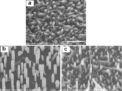
Figure 1: Scanning electron microscope images from the combinatorial library: (a) ZnO wetting layer grown using gold catalyst (note the absence of NWs); (b) ZnO NWs grown using gold-copper alloy catalyst; (c) ZnO NWs grown using silver catalyst. Growth temperature 850 °C. The scale bar on the top image is 1 µm. We have examined the role of elemental noble metals and their alloys on ZnO NW growth and properties. An experimental library was designed using the ternary silver-gold-copper phase diagram and included elemental, binary and ternary compositions as well as two growth temperatures (850 and 950 °C). The metal library elements were deposited on a single gallium nitride/sapphire substrate, which was subsequently annealed to form isolated metal droplets upon which the ZnO NWs were grown. The resulting set of metal islands and ZnO NWs was characterized using electron microscopy, x-ray diffraction, and optical spectroscopy. It was found that the ZnO NW growth was significantly influenced by the nature of the catalytic metal droplets formed on the substrate. For example, growth from the Au islands at 850 °C yielded only a thin ZnO nucleation layer with no NWs, while other metal compositions, which melt at lower temperatures than Au, produced a variety of NW shapes, sizes and orientations at this temperature (Figure 1). A combinatorial approach also permits rapid correlation of the optical properties of the nanowires with the composition of the metal islands from which they were grown. For example, ZnO NWs fabricated from the silver islands at 850 °C produced the sharpest excitonic peak near 3.36 eV on the cathodoluminescence spectrum (comparable to that for bulk ZnO single crystal), indicating superior crystalline structure. In contrast, the spectra were significantly broader for the NWs grown from the gold and copper containing islands. A comprehensive assessment of the correlation of structural and spectroscopic data for the ZnO NW library is still underway. These initial results demonstrate the power of the combined phase diagram/combinatorial approach for controlling semiconductor NW properties.
Contributors and CollaboratorsW. Boettinger, D. Josell, C. Handwerker, U. Kattner, M. Vaudin, I. Levin, L. Robins (MSEL); B. Nikoobakht (CSTL); N. Sanford (EEEL); A. Motayed (University of Maryland) Back to Top
Advanced Processes and Materials for On-Chip InterconnectsAs dimensions of copper wiring in on-chip electrical conductors drop below 100 nm, control of electrical resistivity has become critical. We have demonstrated new barriers for seedless deposition processes that will simplify processing and replace high resistivity tantalum barriers. We have also demonstrated gold superfill as an alternative metallization. NIST Contact: Daniel Josell and Thomas P. MoffatAs dimensions of transistors in integrated circuits shrink, the dimensions of the metal wires connecting them shrink as well. With industry passing through the 90 nm node, electron transport is reduced and fabrication is increasingly difficult.
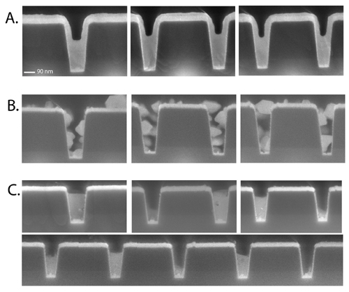
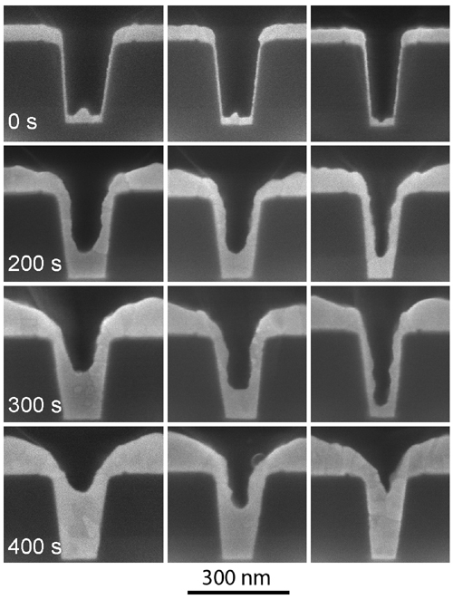
Figure 1: Copper superfill in trenches with ruthenium barriers and no copper seed. (A) Desired copper wetting and superfill. (B) Poor wetting in the presence of surface oxide. (C) Intriguing localized deposition in trenches, the origin of which is unknown. Consistent with dimensional requirements specified in the International Technology Roadmap for Semiconductors, we have been exploring new barrier materials that will permit copper electrodeposition without a copper seed layer. We have explored platinum group elements and have found several that permit seedless deposition. As part of this effort, we have explored in depth the role of oxide removal and underpotential deposition of copper in determining the wettability of ruthenium barriers and associated reliability for seedless copper superfill. This work has demonstrated a process for "repair" of seeds through removal of surface oxide. We have also explored novel metallizations. With the successful demonstration of gold superfill this year (Figure 2), we have now established processes for superfill with three metals, our work being the first to demonstrate superfill with either silver or gold.
Figure 2: Gold superfill in trenches of three different aspect ratios after indicated deposition times, showing bottom-up superfill.
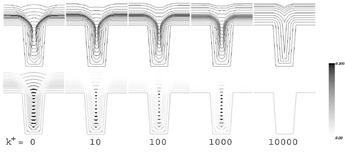
Figure 3: The impact of leveling additives on trench superfill and overfill bump formation. Higher adsorption kinetics k+ leads to reduced overfill bump formation (top), consistent with experimental observation. Corresponding coverage of accelerator is shown beneath. Recognizing the significance of leveling additives in industrial processing, we have now extended our Curvature Enhanced Accelerator Coverage (CEAC) mechanism to account for their presence during superfill. The resulting equations predict reduction of overfill bump through the use of levelers (Figure 3), consistent with observation. Experiments are underway to assess kinetics to permit quantitative comparison to experiment. Contributors and CollaboratorsC. Witt (Cookson-Enthone); D. Wheeler (University of Maryland) Back to Top
Pb-free Surface Finishes: Sn Whisker GrowthSoldered joints are increasingly tenuous links in the assembly of microelectronics as a consequence of ever shrinking chip and package dimensions, the broadening use of flip-chip technology, and the movement toward environmentally friendly lead-free (Pb-free) solders. To support needs in this area, the goal of this project is to provide data and materials measurements of critical importance to solder interconnect technology for microelectronics assembly. NIST Contact: Maureen E. Williams and Kil-Won MoonIt is well known that the use of pure tin protective deposits can lead to problems with whiskers - filamentary whiskers typically 1 �m diameter and several mm long which grow from the plating and cause electrical shorts and failure. Historically, lead was added to tin plate to prevent whisker growth as well as lower costs. The present project focuses on Pb-free, Sn-rich deposits with alloying additions that could potentially retard whisker formation. The Sn-Cu system was selected for compatibility reasons, since Sn-Cu-Ag is likely to be the Pb-free solder of choice for industrial applications. The substitution of a different solute for Pb in the Sn-rich deposit was proposed to also retard whisker growth. A detailed microstructural comparison of deposits with high- and low-whiskering tendency has been conducted, leading to a correlation of Sn grain size, shape, and residual stress with whisker growth. A manuscript submitted to Acta Materialia, Hillock and Whisker Formation in Sn, Sn-Cu and Sn-Pb Electrodeposits, presents measurements of compressive stress in the electrodeposits and how various microstructural features of the deposits affect whisker growth. Relief of the compressive stress occurs by uniform creep for Sn-Pb because it has an equiaxed grain structure. On the other hand, localized creep in the form of hillocks and whiskers occurs for Sn and Sn-Cu because both have columnar grain structures. Compact hillocks form for Sn deposits because the columnar grain boundaries are mobile. Contorted hillocks and whiskers form for the Sn-Cu deposits because the columnar grain boundary motion is pinned by intermetallic precipitates. Some reports suggest that restraining and cracking of a tin oxide surface film are necessary steps in the nucleation of Sn whiskers. However, results at NIST, accepted for publication in the Journal of Electronic Materials showed little support for this mechanism.
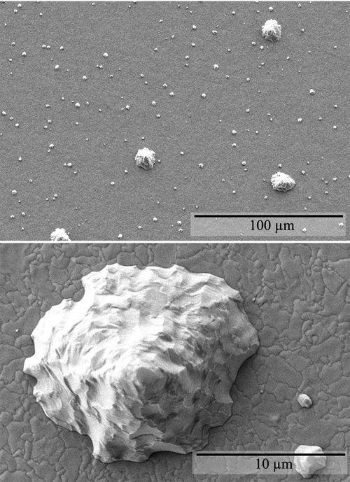
Figure 1: Low and high magnification SEM micrographs of the electrodeposited surface of a 16 �m thick pure Sn layer on a cantilever beam showing bimodal size distribution of conical hillocks. Such hillocks form to relieve compressive residual stress. Whiskers form when grain boundaries in the deposit are pinned by precipitates. For instance, whiskers were observed on bright Sn-Cu electrodeposits but not on pure bright Sn electrodeposits on pyrophosphate Cu substrates. In order to understand the role of the deposit surface, the Sn oxide surface film and surface structures were analyzed by Auger and Electron Backscatter Diffraction (EBSD). In Auger analysis, residuals of the Sn oxide surface film were observed after Ar+ ion cleaning. This feature allowed us to discriminate the Sn whisker growth with or without the oxide surface film. Contributors and CollaboratorsW. Boettinger, C. Johnson (Metallurgy Division, NIST) Back to Top
Nano-Structured Materials for Sensors and Ultra-High Density Data StorageMagnetic sensors play a central role in many important technologies ranging from health care to homeland security. A common need among these technologies is greater sensitivity through nano-structured materials. In ultra-high density data storage, one of the most pressing needs is for nano-structured media that store data at ever-increasing densities. Improved methods for the magnetic isolation of grains in ultra-thin films are a key need. We have initiated research programs in both areas. NIST Contact: William F. Egelhoff, Jr.Over the past decade, NIST's Magnetic Engineering Research Facility (MIRF) has made important and widely recognized contributions to the thin magnetic films used as read heads for hard disk drives. MIRF is one of the most versatile facilities in the world for the fabrication and analysis of novel magnetic thin films. This versatility is illustrated by two new areas of research that have recently been initiated. One is magnetic sensors and the other is magnetic media. The common link is that both require nano-structured thin films.
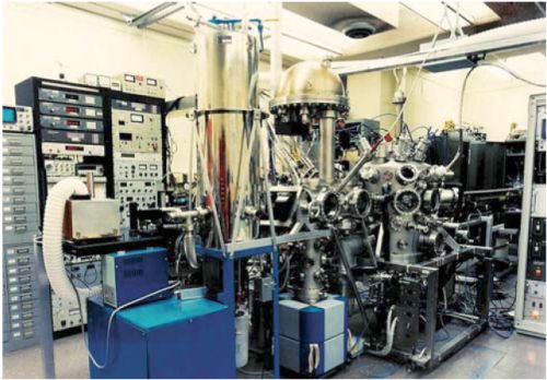
Figure 1: The Magnetic Engineering Research Facility. We are now 1.5 years into the Magnetic Sensors Competence Program. We have evaluated a series of complex magnetic alloys that in bulk form are very sensitive to small magnetic fields but had not previously been studied in thin-film form (e.g., Ni77Fe14Mn5Cu4). Our approach is to carry out the metrology needed to optimize these materials in thin-film form. We have made several surprising discoveries. First, these alloys are uniformly less sensitive in thin-film form. Second, some of the bulk sensitivity can be recovered by nano-layering the magnetic thin films with non-magnetic thin films. Third, conventional thin-films sensor designs contain a design flaw that allows magnetic irregularities to reduce the potential sensitivity by over a factor of 100. Fourth, we have found a way to use nano-structuring of the thin films to reduce these irregularities sharply and achieve a factor of 40 improvement in sensitivity. Fifth, an analysis of the physics of the nano-structuring immediately suggests that opportunities exist for significant further gains. In the area of novel magnetic media we have been collaborating very closely with Seagate. Seagate is the world's leading manufacturer of hard-disk drives, and for the past two years, they have been sending a Ph.D. physicist from their research labs to work with us, first on ballistic magnetoresistance, and then on novel magnetic media.
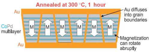
Figure 2: Grains isolated magnetically by Au diffusing into grain boundaries. In recent work, we have found a novel method for magnetically decoupling grains in CoPd media. CoPd multilayers are one of the leading candidates for the next generation of magnetic media. We have found that if we deposit an Au film on top of the CoPd and anneal the sample in air, two unexpected phenomena occur as a result of rapid diffusion of atoms along grain boundaries. One is that Co atoms diffuse to the surface, react with oxygen, and remain at the surface. The other is that Au atoms diffuse into the grain boundaries replacing Co. The net effect is that the grain boundaries are demagnetized, and each grain can magnetically switch independently of its neighbors. This method provides the best magnetic isolation of grains yet found. This work has been reported at several conferences and industrial workshops. Contributors and CollaboratorsE.B. Svedberg, D. Weller (Seagate); R.D. McMichael, T.P. Moffat, J. Mallett, A.J. Shapiro, J.E. Bonevich (Metallurgy Division, NIST); D.P. Pappas (Electromagnetics Division, NIST); M.D. Stiles (Physics Lab, NIST) Back to Top |
|
|
|
Metallurgy Division of MSEL | metallurgy@nist.gov Home | Personnel | Research Opportunities The National Institute of Standards and Technology (NIST) is an agency of the U.S. Commerce Department. Privacy policy / security notice / accessibility statement / Disclaimer / Freedom of Information Act (FOIA) / No Fear Act Policy / ExpectMore.gov (performance of federal programs) / NIST Information Quality Standards |
Last modified: by Metallurgy Webmeister

