Magnetization Dynamics in Films with Nanometer Scale Microstructure
Magnetization damping is essential for data storage and retrieval at GHz data rates in disk drives, MRAM chips and other magnetoelectronic devices. In disk drives, the write head materials, media and read head must all be able to perform well on nanosecond time scales. For measurement of magnetic damping parameters, ferromagnetic resonance (FMR) is the dominant technique, but the raw linewidth data is often clouded by the presence of inhomogeneities. Our modeling of ferromagnetic resonance spectra in inhomogeneous thin films takes a novel approach to a problem that for several decades has been solved only for weak inhomogeneities. Our new model involves solving for the normal modes of an inhomogeneous film and calculating the absorption spectrum from all of the modes. This model provides the theoretical basis for studying the intrinsic damping processes through FMR linewidth measurements, and ultimately for delivering the needed data on magnetic damping to industry.
Magnetic data storage has become the most prevalent form of data storage in the world, far surpassing paper documents in worldwide capacity. Annual hard drive storage capacity shipped is approximately 1 × 1019 bytes with a 60% per year growth rate. To handle anticipated storage at GHz data rates, it is important to understand and control magnetization damping, the process that allows magnetization to come to equilibrium by dissipating heat. To develop high-data-rate hard drives, it will be important to understand and control damping in the magnetic materials used in write heads, media and in read heads. For magnetic random access memory (MRAM) chips, damping is a limiting factor for the speed of these chips because reliable switching of the magnetic “bit” requires waiting for the magnetization to come to equilibrium before the next switching event.
The Nanomagnetodynamics Project is a cooperative project between the Metallurgy Division in MSEL and the Magnetic Technology Division in EEEL. The work is designed to address magnetization dynamics, and magnetization damping in particular, and to deliver to industry the data and metrology needed to develop high-data-rate magnetic devices. This highlight describes a recent theoretical breakthrough by MSEL staff that will enable reliable magnetization damping metrology.
The primary measurement used to determine the damping properties of magnetic materials is ferromagnetic resonance (FMR) linewidth. Ferromagnetic resonance, like electron spin resonance (ESR) and nuclear magnetic resonance (NMR) involves precession of the magnetization around an equilibrium direction at a frequency that depends on the applied field. The damping rate is determined from the width of the susceptibility peak corresponding to the magnetization precession frequency as illustrated in Figure 1.
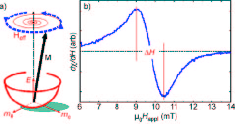
Figure 1. a) Magnetization precession. Damping causes the magnetization to come to equilibrium as shown by the red spiral. b) A typical FMR signal, taken at 2.5GHz in a 10nm thick film of Permalloy. Damping is measured through the line width ∆H.
Measurements of damping in ferromagnetic materials are complicated by the fact that in addition to damping, inhomogeneity contributes to the FMR linewidth. Reliable interpretation of FMR linewidth data therefore requires separation of the linewidth into components arising from damping and inhomogeneity.
Unlike ESR and NMR in paramagnetic materials, the spins in ferromagnetic materials are strongly coupled by short-range exchange interactions and long range dipolar interactions. To account for magnetic interactions, it is convenient to describe the vibrations of the magnetization in terms of spin waves, or in quantum mechanical language, “magnons.” Spin waves (magnons) are the collective vibrational normal modes of the magnetization in a uniform film just as sound waves (phonons) are the collective normal modes of a uniform crystal lattice. The analogy with sound waves is useful in describing the interaction of spin waves with defects. If a sound wave encounters a defect where the elastic properties are different, a portion of the incoming sound energy will be scattered into sound waves traveling in different directions, but with the same frequency. For spin waves, the uniform precession that is driven by a microwave field in an FMR experiment can be scattered into short-wavelength spin waves with the same precession frequency as the uniform mode. The quantum mechanical Hamiltonian describing a system with defects can be written
H = h ∑ ωk
α k†
ak +
h ∑ ( Ak,k'
α k†
α k' +
A * k,k'
α k
α k'† )
where αk†and αk are the magnon (or phonon) creation operators for waves at frequency ωk and Ak,k is a coefficient describing the strength of the defect that produces scattering.
The “two-magnon” model was first derived in the 1950’s to describe the effects of defects on linewidth measurements in bulk ferrite materials. Until the present work, it was the most sophisticated model of inhomogeneities in FMR.
The physical picture presented by the two magnon model is that inhomogeneities cause energy to be transferred from the k = 0 uniform precession mode to other k ≠ 0 spin wave modes having the same frequency. The two-magnon model is expected to be valid when the spin wave amplitudes are small compared to the uniform precession amplitude, so scattering from spin wave modes back to the uniform precession mode is weak and spin wave–spin wave interactions are not important.
Our approach to the problem of ferromagnetic resonance in inhomogeneous thin films treats the very common case where the Ak,k coefficients are too large for the two-magnon model to be valid. To do this, we start with the Hamiltonian for films with inhomogeneities given above and find the eigenmodes and eigenvalues directly. This process involves constructing a model microstructure of the film, calculating the Ak,k' coefficients, limiting the Hamiltonian to approximately 1000 spin wave modes and computationally diagonalizing the Hamiltonian matrix having elements Ak,k + ωkδk,k ´.
The resulting eigenmodes of the inhomogeneous film are mixtures of the spin waves and the uniform, k = 0 precession mode. Each eigenmode has a finite coupling to a uniform driving field that depends on the amount of the k = 0 mode that it contains. Figure 2 shows the eigenmode spectrum and an eigenmode for a typical calculation.
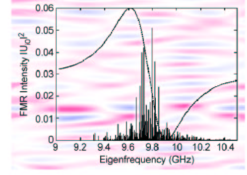
Figure 2: Eigenmode spectrum of an inhomogeneous thin film. Each eigenmode couples directly to the uniform FMR driving field to give the simulated FMR spectrum shown. The background image is the magnetization pattern corresponding to one of the eigenmodes. The image width is 5mm and the defect size is 20nm.
The physical picture presented by this model is very different from that of the two-magnon model.
Inhomogeneities do not merely couple the spin wave modes, they cause mixing of the spin wave modes into a new set of eigenmodes, each of which is observable in an FMR experiment. In this picture, it is clear that the linewidth caused by inhomogeneities is due to a spreading of the FMR intensity in frequency, not to any additional damping process.
Figure 3 shows a comparison between our eigenmode calculation, the two-magnon model and experimental linewidth measurements for a 20 nm film of Permalloy deposited on polycrystalline NiO. The coupling to antiferromagnetic NiO produces an inhomogeneous “exchange bias” field and a uniaxial anisotropy field that varies in strength and direction from grain to grain. These intentionally created “defects” are turned off by deposition of a thin layer of Ta on the NiO, decoupling it from the Permalloy.
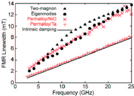
Figure 3: Comparison of the two-magnon model and the eigenmode model of FMR line width with Permalloy films: one made inhomogeneous by NiO and a control sample.
The development of this new model of FMR in inhomogeneous films is important in several respects.
■ It gives a clear physical picture of the magnetization dynamics in inhomogeneous thin films.
■ It clarifies that the linewidth due to inhomogeneities does not constitute a different kind of damping.
■ It provides the theoretical basis for interpreting FMR linewidth that will allow us to study the intrinsic damping processes and, ultimately, to deliver the necessary data to industry.
For More Information on this Topic
For further information on magnetization dynamics, damping and ferromagnetic resonance, please contact R.D. McMichael.
Andrew Kunz and R.D. McMichael, “Normal Mode Mixing and Ferromagnetic Resonance Linewidth.” IEEE Trans. MAG, (in press).
Back to Top
Ballistic Magnetoresistance:
A New Phenomenon with Great Potential for Magnetic Sensors
Magnetic sensors play a central role in many important technologies ranging from data storage to health care to homeland security. A common need among these technologies is higher sensitivity and smaller size. One possible route to higher sensitivity and smaller size is the introduction of the Ballistic Magnetoresistance (BMR) effect as a method of sensing magnetic fields. Although BMR is, at present, a poorly understood and poorly characterized effect, it has shown very large magnetoresistance values in nanoscale devices and could potentially lead to dramatic improvements in magnetic sensors. NIST has initiated a program aimed at clarifying, controlling, and utilizing BMR for advanced magnetic sensor applications.
Magnetic sensors play a central role in many important technologies. To name just a few, computer hard disk drives use magnetic sensors to read stored data, magneto-encephalography uses magnetic sensors to image brain wave activity, and bio-hazard detectors use magnetic sensors to detect magnetic beads that are bio-tagged for biological agents such as anthrax, botulism, and cholera.
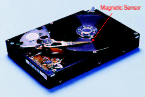
Figure 1: Computer hard disk drives use a magnetic sensor to read data.
A common need among these technologies is sensors with higher sensitivity and smaller size. With higher sensitivity and smaller size, more data could be stored on a hard disk, higher resolution imaging of brain activity would be possible, and earlier warnings of bio-contamination could be given.
The recent discovery of the Ballistic Magnetoresistance effect (BMR) holds the promise of both greatly increased sensitivity and greatly reduced size for magnetic sensors. Figure 3 illustrates how a typical sample is fabricated.
Magneto-encephalography: Imaging Brain Activity
An array of 37 magnetic sensors (left): An image of epileptic activity (right):

Figure 2: Magnetic sensors are the only technology available for real-time imaging of brain activity. Current sensors are bulky and provide low resolution. Advanced sensors could provide much higher resolution and provide improved surgical guidance.
A sharp Ni wire is placed about 20 µm from a flat Ni substrate. In an electrochemical cell, an electrodeposition potential is applied between the wire and substrate. A fine column of Ni grows out from the wire until it meets the substrate. When electrical contact is made between the column and the substrate the electrodeposition potential drops immediately to zero and the electrodeposition stops. At the point of contact with the substrate, the column has a diameter of ~10 nm. When the wire and substrate are magnetized in parallel, electrical current easily flows through the nanocontact. However, when the magnetization is antiparallel, as illustrated in Figure 3, electrons tend to be reflected at the nanocontact because they have the wrong spin to pass easily through this region, and a sharp increase in electrical resistance is observed. This effect is known as magnetoresistance, and values as large as 700% have been observed in this type of magnetic nanocontact.
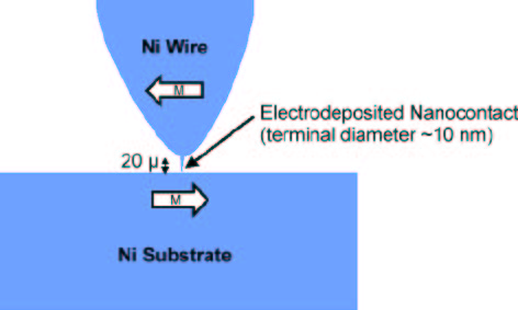
Figure 3: An illustration of magnetic nanocontacts formed by electrodeposition that exhibit very large values of magnetoresistance (N. García, et. al., 2001).
To put this result in context, the sensors that read data from hard disk drives currently have a magnetoresistance of only about 15%, almost 50 times smaller. Moreover, the size of the nanocontact in BMR samples is ~ 50 times smaller than the hard disk drive sensors. Thus, the BMR effect holds the potential for magnetic sensors of greatly increased sensitivity and greatly reduced size.
The term “ballistic” means that the nanocontact is too small for electrons to flip their spin in transit, as they would in a macroscopic Ni sample.
Unfortunately, it often takes many years to go from laboratory demonstration of a concept to a commercially successful device. While BMR looks promising, it is certainly at an early stage of development. The samples investigated so far have poor reproducibility, poor stability, and poor reliability. The techniques of fabrication are poorly understood, and there is no theory that can explain the magnitude of the BMR effect.
Fortunately, there is the precedent of the Giant Magnetoresistance (GMR) effect to serve as a model. When GMR was discovered in 1989, it was subject to very similar shortcomings. Many experts thought it would never be a commercially successful technology. However, the technical community, assisted by a strong effort at NIST, began to address the issues, and gradually the problems were solved. The result is that, today, every hard disk drive produced in the world uses GMR technology in the read head.
Clearly, the sample geometry illustrated in Figure 3 is not suitable for fabrication of hard disk read heads. The industry’s manufacturing practices require lithographic processing on wafers, and a fundamentally different approach would be prohibitively expensive. In light of this need, initial work at NIST has focused on techniques for achieving BMR in planar geometries on wafers. Our first attempt is illustrated in Figure 4. Although the geometry looks ideal, the BMR achieved so far is only 14%. We believe the problem lies in the method of pinhole formation. Consequently, we are exploring novel approaches to controlling pinhole size, such as the use of the Coulomb explosion that occurs when a highly charged ion like Xe44+ contacts a surface. By varying the charge on the ion, the size of the pinhole can be finely tuned.
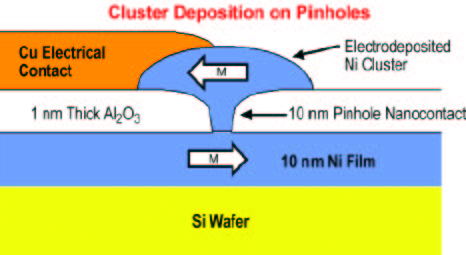
Figure 4: A planer geometry for BMR. Pinholes are created by dielectric breakdown at thin spots in an Al2O3 film when the electrodeposition potential is applied.
A different and much more successful planar geometry on a wafer is illustrated in Figure 5. In this work, a Ni film ~10 nm thick is deposited on an insulating wafer and patterned into the form of a nano or micro gap. Electrodeposition is used to bridge the gap with a Ni nanocontact. In such samples, we have been able to achieve a much higher BMR value of 350%. However, problems with reproducibility, stability, and reliability remain. We are investigating these shortcomings with scanning electron microscopy (SEM) with polarization analysis, transmission electron microscopy (TEM), Lorentz microscopy, and scanning tunneling microscopy (STEM). The field of BMR is so new that very little microscopy has been carried out to date.
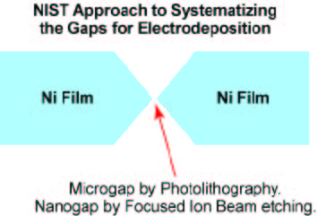
Figure 5: An illustration of Ni films with lithographically patterned gaps for electrodeposition of magnetic nanocontacts on wafers.
We believe that with these studies, it is likely that the shortcomings of BMR materials can be addressed, and BMR technology can move towards a new generation of ultrasensitive nanoscale magnetic sensors that will have wide-ranging impact on many important technologies.
“The technical challenges facing the data storage industry in the next 10 years are so broad and so deep that the industry cannot do it alone. Weneed researchers like you here at NIST to help us.”
Dr. Sining Mao
Director, Read-Head Research
Seagate Technology
June 14, 2002
For More Information on this Topic
Contact: W.F. Egelhoff, Jr.
M. Muñoz, G.G. Qian, N. Karar, H. Cheng, I.G. Saveliev, N. García, T.P. Moffat, P.J. Chen, L. Gan, and W.F. Egelhoff, “Ballistic Magnetoresistance in a Nanocontact between a Ni Cluster and a Magnetic Thin Film.” Appl. Phys. Lett., 79, p. 2946, (2001).
Back to Top
Advanced Metallizations for Sub-100 Nanometer Electronics
Electrodeposited copper is rapidly replacing aluminum in device interconnect technology because of its lower electrical resistivity, superior electromigration behavior, and the ability to fill fine features without the formation of seams or voids. As feature dimensions go below 100nm difficulties in maintaining performance are anticipated. In FY2002 we have pushed the quantitative limits of the Curvature Enhanced Accelerator Coverage (CEAC) mechanism developed in the Metallurgy Division of NIST. Exploring the mechanism has yielded new electrochemical processing routes for improved metallization and is guiding the development of advanced metallizations beyond copper as well as new processing routes such as surfactant catalyzed chemical vapor deposition.
This Metallurgy Division project is meeting the microelectronics industry’s need for improved device metallization by exploring advanced materials and processes for superconformal film growth. In FY2002 we have:
■ Established the generality of the CEAC model for superfilling by electrodeposited silver and other metals;
■ Developed a new processing method for eliminating the delay time for superfill to begin during electrodeposition, thereby increasing the aspect ratio and decreasing the width of trenches that can be superfilled; and
■ Extended the CEAC mechanism to quantitatively predict superfill during chemical vapor deposition.
Our current measurement and modeling effort is focused on copper and silver metallizations, the latter metal having the lowest resistivity of any element, thus having potential on-chip applications. Superconformal silver deposition was demonstrated this year in the Metallurgy Division and is the first example of superconformal feature filling with a metal other than copper. “Superfilling” is characterized by bottom-up deposition as shown in Figure 1.
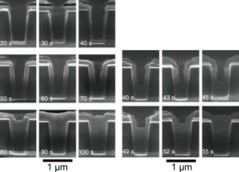
Figure 1: Superconformal filling of vias during silver (left) and copper (right) electrodeposition (NIST Metallurgy Division, using patterned wafers from International SeMaTech).
Filling of trenches and vias with silver and copper is quantitatively explained by the Curvature Enhanced Accelerator Coverage Mechanism (CEAC) developed at NIST. Electrochemical and surface analytical measurements on planar substrates were used in FY2002 to establish a one-to-one correlation between catalyst coverage and the metal deposition rate. In the case of silver deposition, adsorbed selenium was found to catalyze the deposition rate. For the thiol /disulfide-polyether-halide additives used in copper superfilling, the sulfonate-end group of the thiol or group of the thiol or disulfide molecules was found to destabilize the passivating polyether surface film thereby accelerating the local metal deposition rate.
The insight provided by uncovering the CEAC mechanism has enabled the development of a new two-step process for superconformal film growth; in contrast to standard electrodeposition techniques, the catalyst is deposited on the substrate prior to the metallization. Specifically, the patterned substrate is first “derivitized” or “dosed” with a submonolayer coverage of catalyst and then transferred for electroplating in an electrolyte that does not contain the catalyst. For an optimum catalyst coverage, superconformal filling of trenches and vias occurs as shown in Figure 2 (50 µmol/L SPS). If the catalyst coverage is too low or high, conformal or subconformal deposition occurs, resulting in void formation during feature filling (0.5, 500 µmol/L SPS, 1mmol/L MPSA). The filling behavior is completely analogous to that obtained using a single (conventional) electrolyte containing both catalytic and inhibiting species. The new process provides unambiguous verification of the CEAC mechanism of superconformal film growth. Restricting the catalyst to the surface prior to metal deposition also enables the rate differentiation provided by the CEAC mechanism to be increased relative to the conventional process. From a technical perspective, the two-step process offers an interesting solution to the difficult control issues associated with catalyst destruction and related aging effects which are known to occur in the “conventional” single-electrolyte superfilling process currently used in industry.
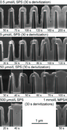
Figure 2: Time evolution of trench filling after different “derivitization” steps. The concentration of SPS or MPSA catalyst used for the 30s surface derivitization steps are indicated. All specimens were transferred to a catalyst-free electrolyte for copper deposition.
The generality of the CEAC mechanism has now been extended to include the first quantitative prediction of superconformal chemical vapor deposition (CVD). More recently, this work has enabled a direct comparison of the CEAC mechanism with detailed experiment results on iodine catalyzed copper CVD as shown in Figure 3.
Project results from FY2002 have firmly established the generality of the Curvature Enhanced Accelerator Coverage (CEAC) mechanism, which we developed in FY2001 to explain superconformal electrodeposition of copper. The output also clearly demonstrates the predictive power of the CEAC formalism.
Three different electrode-shape change algorithms have been developed. They show excellent agreement with experimental results.
These algorithms, in the form of software, are available from the Metallurgy Division website and are currently being examined by Texas Instruments and IMEC. In addition, Motorola (B. Melnick and M. Freeman), International SeMaTech (C. Witt) and
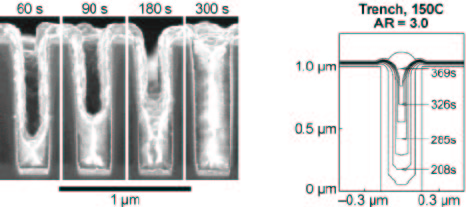
Figure 3: Superconformal filling of vias during iodine catalyzed chemical vapor deposition. Experimental via results are from Hynix Semiconductor, and model predictions for a trench are from the Metallurgy Division of NIST.
Hynix Semiconductor (S.G. Pyo) are now active collaborators in our experimental and modeling efforts. The first two provide patterned wafers for NIST electrodeposition studies; the last provides results from iodine catalyzed chemical vapor deposition experiments for NIST modeling.
Selected Project Publications for FY2002
D. Wheeler, D. Josell and T.P. Moffat, Modeling Superconformal Electrodeposition Using the Level Set Method, J. Electrochem. Soc., submitted July 2002.
T.P. Moffat, D. Wheeler, C. Witt and D. Josell, Superconformal Electrodeposition Using Derivitized Substrates, Electrochemical and Solid-State Letters, submitted May 2002.
D. Josell, S. Kim, D. Wheeler, T.P. Moffat, S.G. Pyo, Superconformal Deposition by Iodine-Catalyzed Chemical Vapor Deposition, J. Electrochem Soc., submitted May 2002.
B.C. Baker, M. Freeman, B. Melnick, D. Wheeler, D. Josell, T.P. Moffat, Superconformal Electrodeposition of Silver from a KAg(CN)2-KCN-KseCN Electrolyte, J. Electrochem. Soc., in press.
D. Josell, B. Baker, C. Witt, D. Wheeler and T.P. Moffat, Via Filling by Electrodeposition: Superconformal Silver and Copper and Conformal Nickel, J. Electrochem. Soc., in press.
T.P. Moffat, B. Baker, D. Wheeler, J.E. Bonevich, M. Edelstein, D.R. Kelly, L. Gan, G.R. Stafford, P.J. Chen, W.F. Egelhoff, and D. Josell, Superconformal Electrodeposition of Silver in Submicron Features, J. Electrochem. Soc. 149, C423 (2002).
D. Josell, D. Wheeler and T.P. Moffat, Superconformal Electrodeposition in Vias, Electrochemical and Solid-State Letters 5, C49 (2002).
D. Josell, D. Wheeler and T.P. Moffat, Superconformal Deposition by Surfactant-Catalyzed Chemical Vapor Deposition, Electrochemical and Solid-State Letters 5, C44 (2002).
D. Josell, D. Wheeler, W.H. Huber, J.E. Bonevich and T.P. Moffat, A Simple Equation for Predicting Superconformal Electrodeposition, J. Electrochem. Soc. 148, (12) C767 (2001).
Our findings have also been conveyed to U.S. industry, academia and other national laboratories through more than ten external presentations in the last year.
For More Information on this Topic
D. Josell, D. Wheeler, B. Baker, T.P. Moffat
Back to Top
Performance-Limiting Defects in GaN
The III-V nitrides and GaN, in particular, are emerging new semiconductors for electronic devices, including light-emitting diodes (LED) and laser diodes in the blue-green and UV wavelengths, UV detectors and ultrahigh power switches. The main challenges in this technology are optimization of optical output efficiency and stability of metal contacts. One objective of the MSEL project on GaN is to quantify the effect of GaN defects, in particular of threading dislocations, on these properties. In FY2002 a mechanism for the degradation of electrical contacts through threading dislocation-mediated phase transformations was determined through detailed characterization using transmission electron microscopy. Doping methods to disable the mechanism may lead to greatly improved stability,reliability, and performance of commercial GaN devices.
Direct bandgap GaN and its alloys with AlN and InN are receiving considerable attention as promising semiconductors for electronic devices operating at high temperatures, high frequency and high power and for optoelectronics applications in the blue-green and UV wavelengths. Therefore, electrical contacts to the nitrides (ohmic contacts and Schottky barriers) which are stable at elevated temperatures are needed.
As bulk crystals of these materials are not available, GaN is epitaxially grown on a substrate, usually on (0001) sapphire or (0001) 6H-SiC. Because of a large lattice mismatch between the substrates and GaN, high densities of various crystallographic defects are present in the active GaN layers. Among the defects that can cross the epitaxial GaN layer and reach a surface are threading dislocations, inversion domains, nanopipes and prismatic planar defects.
In order to achieve desirable characteristics of ohmic contacts, different combinations of different metal layers have been studied. For example, the commonly accepted contact to p-type GaN is Ni /Au which gives good electrical characteristics after annealing at 400-600°C. For higher temperatures, the electrical characteristics worsen and severe degradation of contact morphology is observed. Degradation of such electrical contacts are associated with dislocations in GaN, island formation in the contact layers, and decomposition of GaN. In FY2002, NIST developed a mechanism for contact degradation that is based on heterogenerous nucleation of GaN decomposition at threading dislocations/metal interface, followed by wetting of the threading dislocation by liquid Ga. The morphology of the metal/ GaN interface is an important issue: if the Ga metal were to penetrate through a thin GaN layer and reach an underlying layer in a device, the device could be rendered inoperable. Furthermore, the stability of interfacial morphology is a general concern for contacts to all semiconductors.
Reaction and interdiffusion in the Au/Ni/GaN system as a function of annealing temperature from 400 to 900°C has been investigated by several groups, mostly using Rutherford backscattering (RBS), Auger spectroscopy and x-ray scattering. Only rarely has this microstructural evolution been directly observed using transmission electron microscopy (TEM). In collaboration with researchers from the Electrical Engineering Department at Howard University, we investigated electrical and microstructural behavior of Ni/Au bilayers as a function of annealing temperature, with emphasis on structural evolution at a TEM level. The as-deposited layers consisted of 50 nm of Ni and 35 nm of Au, with Ni in contact to n-type GaN. Ohmic contacts with a specific contact resistivity, ρs, as low as 6.9 × 10- 6 Ω-cm2 for a doping level of 5.0 × 1017 cm-3 were obtained after annealing the sample for 10 s at 800°C. Two very important conclusions were achieved from the TEM investigation:
1. A strong reaction between the metal contact layer and the threading dislocations core structure leads to decomposition of GaN along dislocation lines. Such behavior will be a major factor limiting annealing temperature and operation temperature/time of devices.
2. Interdiffusion between Ni and Au results in reversal of Au and Ni phases across the metal film. Thus, after annealing the phase primarily responsible for the formation of the energy barrier of the contact between GaN and metal contact is Au-based.
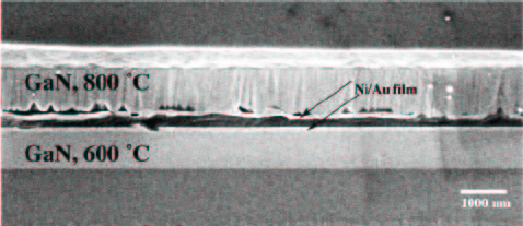
Figure 1: SEM image of Au/Ni/GaN/sapphire annealed at 600 and 800°C for 10 sec.
Figure 1 shows a SEM image of Au/Ni/GaN annealed at 600 and 800°C for 10 sec. For the imaging, we used a cross-sectional ion milled TEM specimen where two differently annealed specimens were glued face to face. Whereas at 600°C the metal film is continuous, at 800°C severe degradation of the metal contact occurred. In many places the film is separated from GaN, and deep V-shaped pits can be found penetrating GaN. Such pits are detrimental to the near-surface electrical performance of devices.
TEM analysis of these specimens showed that the V-shaped pits are always associated with the threading dislocations. Figure 2 shows bright and dark field images of the 600°C-annealed specimen. The pits are clearly seen in the bright field image and marked by triangles. The weak beam imaging using different g-vectors established that each pit is connected to a place where a threading dislocation exits GaN. The threading dislocations vary in character (e - edge, s - screw and m - mixed).
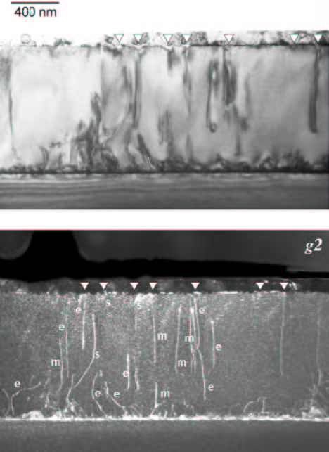
Figure 2: Bright field (upper) and weak-beam dark field (bottom) images of the 600°C-annealed specimen.
Bright and dark field images of the 800°C-annealed specimen are shown in Figure 3. The pits associated with the threading dislocations in the specimen are significantly deeper and wider. The metal film in some places is lifted from the GaN surface, and in other places, the surface of GaN is exposed. It appears that the surface of GaN, between the dislocations, was not degraded and remained flat (see arrows in Figure 3).
This phenomenon, the elevated temperature chemical instability of GaN defects exposed to either metal films or free surfaces, is very general in nature and has importance for GaN-based device design. Bulk GaN has the following decomposition reaction above 800°C: GaN 6 Ga(l)+N2(g). Nevertheless, GaN films can survive higher temperatures due to the high stability of the (0001) surface. In addition, the reaction is sluggish due to kinetic difficulties recombining nitrogen atoms into N2 molecules on the GaN surface. At locations where a dislocation exits GaN, the atomic arrangement is of lower stability and therefore triggers the decomposition of GaN (Figure 4). Nitrogen atoms may diffuse into the metal, recombine into molecules and form N2 gas. Such gas accumulates under the metal film and exerts enough pressure to cause metal film de-cohesion (see Figure 3).
Figure 3: Bright field (upper) and weak-beam dark field (bottom) images of the 800°C-annealed specimen.
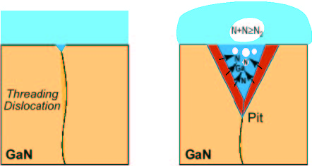
Figure 4: Schematic drawing illustrating decomposition of GaN along a dislocation line and resulting in the formation of N2.
For More Information on this Topic
L.A. Bendersky, A.V. Davydov, W.J. Boettinger
Back to Top
Responding to the Auto Industry’s Research Needs in Materials:
Forming of Lightweight Materials
In response to a recommendation by the NIST Visiting Committee on Advanced Technology, the Industrial Liaison Office (ILO) was established to address the desire of NIST Senior Management for NIST to “close the loop with industry.” In particular, although NIST receives excellent recognition for its work from industrial project leaders and bench level scientists and engineers, at higher levels of industrial R&D management, the impact of NIST’s work is frequently unknown. Since the automotive industry,one of NIST’s largest “customers,” was chosen as a targeted sector, several projects within the MSEL Program on Forming of Lightweight Materials for Automotive Applications were selected to test the industry feedback process and answer the question: “Arewe meeting industry’s needs?” The feedback results were overwhelmingly positive.
The NIST Industrial Liaison Office (ILO) chose three projects within the Metallurgy Division to assess the impact of NIST Laboratory Programs on the auto industry:
■ Standard Test Method Development for Sheet Metal Forming
■ Microstructural Origins of Surface Roughening and Strain Localization
■ Process Models for Metal–Matrix Composites
Detailed descriptions of the first two projects are contained in this annual report. The project on Process Models for MMCs was completed last year and was described in the FY01 annual report.
The ILO process began with the development of surveys that were targeted for a cross-section of researchers, managers, and directors in the automotive and associated industries. The surveys contained brief descriptions of the projects and provided web sites with more detailed project results. At this point, the respondents were queried as to their familiarity with the projects and whether the intended outputs were useful to their companies. A series of questions was designed to assess the impact of the projects on the automotive industry. Finally, the survey sought feedback as to whether some modifications to the projects or any other research would be more valuable than the current projects.
A list of potential industrial contacts was made for each project consisting of researchers, managers, and executive level staff from the appropriate companies. The ILO manager then contacted these individuals and requested their participation in the survey. The surveys were sent out only to those who agreed in advance to provide feedback to NIST. The ILO manager again contacted each individual to go over the survey. For the three projects mentioned, more than 50 surveys and interviews were completed.
Figure 1: A transmission fluid pump component showing centerline porosity (light band) predicted using process modeling shown in Figure 2.
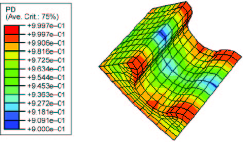
Figure 2: Predicted density of the powder part which is shown in Figure 1. Note low density regions in the middle.
Results of Surveys
Standard Test Method Development for Sheet Metal Forming
Objective: Enable the production of more accurate dies for auto body parts.
Approach: Produce, measure, and analyze multi-axially strained sheet samples.
Product: New standard tests and metrology to accurately determine sheet metal mechanical response under forming conditions.
Relevance: Enables use of lighter, high strength materials required to meet fuel efficiency goals.
Industry Response: The survey revealed that this project is already known and appreciated by a significant portion of the appropriate people in the auto industry. Its uniformly high scores for impact, value of output, and importance indicate that it would be mutually beneficial to extend this awareness to an even greater portion of the industry. The reviewers provided a list of potential new contacts. The addition of these new contacts to future communications by NIST researchers with the automotive industry will help expand the visibility of this project.
Impact of Survey on NIST: Following these surveys, the results were reviewed with the NIST researchers, the Group Leader, the Metallurgy Division Chief, and the MSEL Director. As a result of the survey, the NIST research team has been able to: (1) validate their priorities for materials to be tested, (2) reinforce the current priorities, (3) identify 13 new contacts, (4) learn of the desired form of communicating project results, (5) learn more about types of standard testing that already exist in industry, and (6) identify important future directions.
Figure 3: A pre-standard cup test specimen used at NIST to measure formability and constitutive behavior under equibiaxial strain conditions.
Microstructural Origins of Surface Roughening and Strain Localization
Objective: Develop measurement methods, models, and data that enable industry to predict the behavior of sheet metal in dies.
Approach: Explore the origins of inhomogeneous deformation and its quantification and behavior prediction for use in finite element codes.
Product: Microstructural and formability databases for aluminum and steel.
Relevance: By better understanding the interplay of the material and the stress states encountered within the die, the die tryout period can be reduced and significant cost savings realized.
Industry Response: The response was extremely positive. About 2/3 of the respondents were already aware of the project. Those who were not previously aware of this work became interested as they learned about it. The expected outputs were all considered to be useful and valuable. The window of opportunity was thought to be 12 months. Respondents felt the work was important and that NIST’s assessment of its impact was valid. Only minor modifications were suggested. In particular, high-strength steel and advanced high-strength steel were mentioned as additional alloys of industrial interest. They are eager to establish communications with NIST to follow the progress of this project. The respondents supplied a number of new contacts.
Impact of Survey on NIST: The NIST research team will include several new steel alloys in the project. They also intend to communicate their results directly to the 13 new contacts identified during this process.
Process Models for Metal–Matrix Composites
Objective: Provide process models for the USAMP project “Low Cost Powder Metallurgy Technology for Particle Reinforced Aluminum (PRA)” to accelerate the introduction of PRA into auto parts and to capture the knowledge generated by the USAMP project in a readily usable form.
Approach: Provide models for lightweight metal consolidation, measurements and data for model validation, software that readily transfers the models, and data required to implement the models.
Product: Models and input data for commercial software.
Relevance: Enables use of lighter, high-strength materials required to meet fuel efficiency goals.
IndustryResponse: A limited number of responses were received, perhaps due to the fact that this project was already completed. “Expected outputs” were rated 4.3 out of 5, indicating high value. Three-quarters of the respondents agreed with NIST’s assessment of the project’s impacts and importance. Additional impacts were identified by the respondents. No modifications were suggested, but suggestions for future related projects with details were made.
Impact of Survey on NIST: An interesting issue was raised by the survey. A respondent who knew and approved of NIST’s work did not understand that the modeling software developed by NIST and its partners is broadly applicable to powder consolidation of a wide range of alloys and conditions, not just those of direct interest to the USAMP project. Scientists sometimes assume that the generality of their work is understood; this is a communication issue that must be addressed in order to ensure the greatest impact and application of technical developments.
For More Information on this Topic
Standard Test Method Development for Sheet Metal Forming and Microstructural Origins of Surface Roughening and Strain Localization: T. Foecke, S. Banovic; Process Models for Metal Matrix Composites: R. Fields; NIST Industrial Liaison Office and the impact of these projects on industry:
Back to Top
Thermodynamic Database for Multicomponent Alloys
Commercial alloys rarely consist of only two elements and some contain up to 10 elements. Thermodynamic modeling allows the prediction of phase equilibria in multicomponent alloys from the extrapolation of the thermodynamic descriptions of the constituent binary and ternary systems. Different properties of a system, such as phase boundaries and enthalpies are described with one set of functions resulting in a consistent description of phase properties. The approach gives reasonable predictions for complex alloys, thereby providing a powerful tool for alloy design, and provides a compact storage method for large amounts of phase diagram and other thermodynamic data.
During the last decade, researchers from the Metallurgy Division have collaborated with scientists from universities and industry on several projects with emphasis on modeling tools for the design and manufacture of multicomponent alloys. The traditional approach for development of a new alloy relies on the knowledge and experience of the engineer, which can be costly due to the significant amount of testing required to obtain the correct properties.
Structural parts made from Ni-base superalloys not only must withstand extended periods of service at high temperatures, but also must tolerate severe environmental conditions, such as the highly corrosive environment of a jet engine. Higher operating temperatures result in increased performance demands for both aerospace applications, as well as land-based energy applications.
For a number of projects, including the NIST-sponsored Consortium on Casting of Aerospace Alloys, the DARPA sponsored Investment Casting Cooperative Arrangement, and the General Electric-lead DARPA project for Accelerated Insertion of Metallic Structural Materials (AIM), the Metallurgy Division has constructed a thermodynamic database for Ni-base alloys. The NIST Ni-superalloy thermodynamic database includes 10 elements, Ni-Al-Co-Cr-Hf-Mo-Re-Ta-Ti-W, and is based on critically-evaluated literature and NIST work. Phase equilibria can be calculated from this database. Since the immediate goal for the application of this database was for the modeling of single crystal alloys, the final refinement of the description in the database was restricted to the liquid, fcc-γ and L12-γ´ phases. Figure 1 shows the comparison of experimental liquidus, solidus and solvus temperatures and those predicted from the calculation for a series of commercial superalloys. Experimental and calculated phase boundary data for the γ-γ´ two-phase region are compared in Figure 2.
As a result of this work, detailed solidification behavior for Ni-base superalloys can be predicted. This improved the quality of solidification simulations for investment castings by providing more reliable predictions of casting defects allowing industry to eliminate the need for extensive testing of a series of castings to reach an acceptable design.
In addition to a dependence on the multicomponent thermodynamics, a wide variety of Ni-base superalloy applications are controlled by diffusion processes including solidification, homogenization, γ´ precipitation, bonding and repairing processes, and protective bond coats. Many of these industrial problems can be addressed using a diffusion simulation code that combines composition-dependent diffusivities with multicomponent thermodynamics. The thermodynamic database was used for the development of a diffusion mobility database for Ni-base superalloys. The NIST mobility database can be used in conjunction with the NIST Ni-superalloy thermodynamic database, as well as with other commercial thermodynamic databases.
Electronic versions of the NIST databases have been distributed to various industries, universities, and national laboratories.
Most databases that are currently available to scientists, engineers and students need to be expanded and improved. A workshop on “Databases for Computational Thermodynamics and Diffusion Modeling” was held at NIST Gaithersburg, March 21–22, 2001. The workshop format was a series of invited talks given to the group as a whole followed by general discussions of needs and benefits. The workshop was attended by 39 registered participants of which 16 were from industry. Of the 17 oral presentations given, 8 were from industry, emphasizing the applicability of the modeling approach to industrial processes. Extensive discussions followed the presentations.
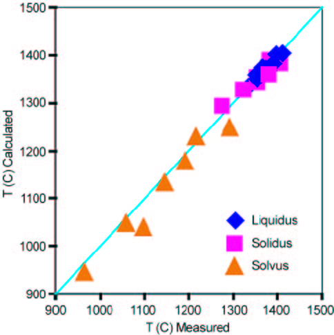
Figure 1: Comparison of experimental and calculated liquidus, solidus and solvus temperatures of superalloys.
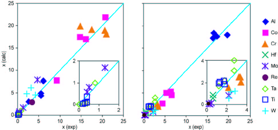
Figure 2: Comparison of experimental and calculated phase boundary data for the γ-γ´ two phase region.
The participants at the workshop agreed that, by the year 2010, it is highly likely that all Materials Science and Engineering students will learn to solve real world materials problems using modeling and simulation tools. The national benefits of providing materials engineers with software and databases for modeling materials and processing are savings in costs, energy and natural resources via optimization studies, as well as improved materials properties and development times. The primary deliverables of the workshop were, first, to identify the database and information delivery tool needs of industry and, second, to propose a roadmap for how these needs can be met.
Expanded collaborative efforts are needed in areas of materials education, basic research, and database development within the next decade to meet these needs. Working groups will be formed for each of these areas in FY2003. The primary objective for materials education identified at the workshop is to interest faculty and students in applied thermodynamics and kinetics by preparing a collection of applied problems. The current NSF program at Penn State University on computational thermodynamics and kinetics will serve as a model for improving abilities of students in these research areas. Basic research was identified to be of crucial importance to generate experimental, as well as calculated data from first-principles calculations. This requires a broad initiative to rebuild the thermodynamic and kinetic measurement infrastructure and to encourage theoretical a priori studies. The action items identified for public databases include encouragement of journal policies to require publication of parameters in assessment papers, recommendation and publication of a data format designed for portability of the thermodynamic parameters and fostering industrial user groups to identify software needs.
The second major activity for FY2002 was developing a relationship with SGTE (Scientific Group Thermodata Europe), one of the leaders in the world effort to develop thermodynamic databases for inorganic and metallurgical systems and their applications to practical, industrial problems. SGTE was originally a consortium founded by European centers active in database development. Today membership in SGTE is no longer limited to European organization and the NIST is being welcomed into the now international group. The aims of SGTE are the critical assessment and compilation of self-consistent thermodynamic data for both pure substances and solutions of all types. SGTE has pioneered the development of multicomponent databases. This includes compilation of the Gibbs energies of the pure elements, published by SGTE in 1991, thermodynamic properties of stoichiometric inorganic compounds in 1999 to 2001 and the planned publication of databases for binary systems. The self-consistency of the SGTE databases has made the thermodynamic quantities and model descriptions de facto standards for the construction of databases for multicomponent systems. Joining SGTE will enable NIST to contribute to the discussion of future model choices and cooperate in the broader international effort to unify thermodynamic data.
For More Information on this Topic
U.R. Kattner, W.J. Boettinger, C.E. Campbell (NIST/MSEL)
U.R. Kattner, CALPHAD and Alloy Thermodynamics, eds. P.E.A. Turchi, A. Gonis, and R.D. Shull, “Construction of a Thermodynamic Database for Ni-base Superalloys: A Case Study.” TMS, pp. 147–164, 2002.
Back to Top