
Metallurgy Division Publications - NISTIR 6797
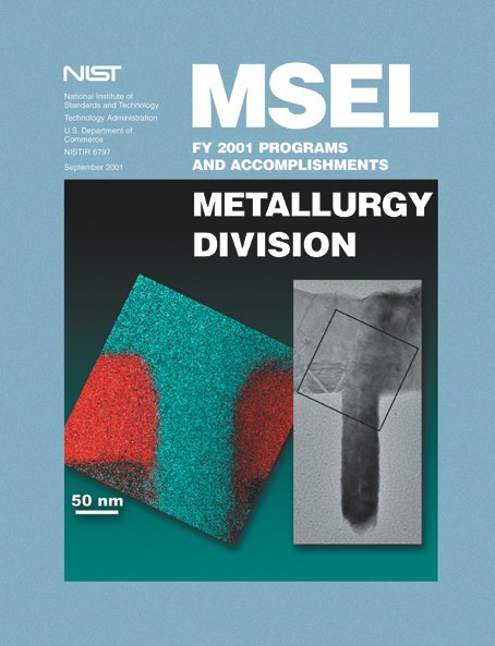
About the Cover Graphic |
|
Cross-section of a nanoscale trench (dimensions of 90 nm wide and 500 nm high), fabricated with an initial seed layer of copper, later filled with electrodeposited nickel. Transmission electron microscopy and compositional mapping reveal salient features on the nanometer scale: electron energy loss spectroscopy was used to generate a compositional map (left), where the red color indicates copper and blue denotes the nickel region. The cross-sectional TEM image (right) reveals microstructural features (note the planar twins in the copper seed layer). Such information supports the development of new electrodeposition metrology techniques for micro- and nano-electromechanical devices (MEMS/NEMS). |
|
|
|
Metallurgy Division of MSEL | metallurgy@nist.gov Home | Personnel | Research Opportunities The National Institute of Standards and Technology (NIST) is an agency of the U.S. Commerce Department. Privacy policy / security notice / accessibility statement / Disclaimer / Freedom of Information Act (FOIA) / No Fear Act Policy / ExpectMore.gov (performance of federal programs) / NIST Information Quality Standards |