|
The following Technical Highlights section includes expanded descriptions of research projects that have broad applicability and impact. These projects generally continue for several years. The results are the product of the efforts of several individuals. The Technical Highlights include:
• Solidification in the Presence of Impurities: Phase Field Simulations of the Growth of “Dizzy” Dendrites
• Advanced Metallizations for Sub-100 Nanometer Electronics
• High Throughput Data Analysis of Multicomponent Multiphase Diffusion Data
• Modeling Dynamics, Damping and Defects for Perpendicular Magnetic Recording Media
• Artifacts in Ballistic Magnetoresistance Measurements
• Phase Field Modeling of the Electrochemical Interface
• NEMI–NIST–TMS Workshop on Tin Whiskers: Cause and Effect
• Kolsky Bar: Materials Properties at High Strain Rates and High Heating Rates
Solidification in the Presence of Impurities:
Phase Field Simulations of the Growth of “Dizzy” Dendrites
It is beyond the capacity of conventional models of solidification to describe and predict the formation and growth of polycrystalline structures. With the NIST development of a new phase field model of polycrystals, entire classes of microstructure are now subject to study not only within the confines of the laboratory but also the theoretician’s computer. This computational tool offers unprecedented control in the design of crystalline and semi-crystalline material.
NIST Contact: James A. Warren and Jack Douglas
During solidification, materials do not freeze in a uniform manner, except under very special circumstances. Instead, a whole host of patterns emerges, of which the snowflake is the most familiar. The snowflake is not unique to water, however, as nearly all materials can solidify having such a pattern, and this process is referred to as dendritic growth. Dendrites, Latin for “trees,” are ubiquitous in solidification and occur in situations from commercial castings to frost on a windshield.
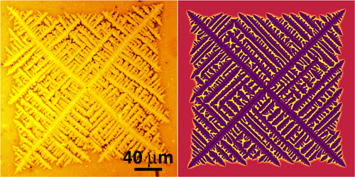
Figure 1: The growing PEO-PMMA polymer dendrite on the left exhibits the four symmetry of the underlying crystal, while the phase field simulation on the right shows striking similarities in its growth form.
Classical studies of solidification consider the growth of a crystal from a nucleus, and, in the absence of other effects, this crystal will have a single crystallographic orientation. Thus, as is shown in Figure 1, symmetry reflecting the underlying four-fold crystal-lattice symmetry is evinced in the growth shape. Indeed, the left figure shows the growth of an undercooled polymer blend (PEO-PMMA) crystallizing in a dendritic pattern with four main branches and a network of fine side branches. The phase field simulation on the right matches this growth form quite well. While the simulations are two-dimensional, the polymer films are thin enough that this is a reasonable approximation.
While such dendritic growth patterns are common, under certain circumstances dendrites can grow which appear to not reflect the underlying crystallographic symmetries, and often, the branches of these dendrites curve in a seemingly erratic fashion. We have termed these growth structures “dizzy dendrites,” and two exemplary experimental results are shown in Figures 2a and 2b. One of the keys to the creation of such growth structures is the presence of clay nucleating agents in the polymer blend, and it has been hypothesized (based on the observation of dendrite tip deflection as it traversed such an impurity) that the presence of these nucleating agents was causing the observed “dizziness.”
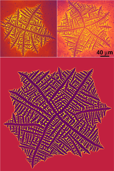
Figure 2: The growing PEO-PMMA polymer dendrites in the upper two images exhibit what we have termed dizzy dendritic growth. The simulation in the lower image is again provocatively similar in its growth form.
However, the very fact that the dendrite no longer reflects the symmetry of the underlying crystal immediately requires that the dendrite no longer be a single crystal, and, thus, a more complex phase field model which incorporates multiple grain orientations is required if we are to describe and predict this interesting phenomenon.
Over the past few years, Metallurgy Division scientists, in collaboration with researchers at MIT and Hokkaido University, have developed a phase field model that extends the models of solidification to include polycrystalline growth. As is often the case in scientific research, the ultimate uses of this model are not those necessarily anticipated by the model developers. In this case, researchers at the Research Institute for Solid State Physics and Optics in Budapest collaborated with NIST scientists to harness this model to explain the observed dizzy dendrites.
Specifically, we have postulated the presence of impurities that, upon incorporation into the solidifying crystal, may cause the creation of a grain boundary. We modeled these impurities by assuming a small region of space has a crystal orientation that is fixed (or has a predetermined orientation as a function of time). We refer to these regions of fixed orientation as pinning centers. Among the many interesting observations found during the evaluation of this model, by numerical experiments, we observed that the dendrites would not typically deflect from their original trajectory unless the tip of the growing stalk crossed very near a pinning center. Studies were also made of the sensitivity of the deflection as a function of the size and misorientation of the pinning center. Finally, we considered a random orientation distribution at a density chosen to be the same as the experimental value for clay nucleating agents in the PEO/PMMA experiments shown in Figure 2. When the simulation was performed, the microstructure had a strong resemblance to experimental observations, as is seen in Figure 2c.
Having successfully modeled the growth of this complex pattern, we now are investigating the possibility of using our increased understanding of these systems to control the types of microstructure that can be created. With that in mind, we explored how the manipulation of included pinning centers can influence the growth shape of dendritic patterns. In Figure 3, we show two such experiments, indicating both the solute distribution (on the left) as well as the crystallographic orientation (on the right). In the upper simulation, we laid down 11 horizontal lines of fixed orientation. This resulted in a main dendrite stalk that zigzagged, while changing orientation to reflect the choices made by the pinning lines. In the lower simulation, we placed a random distribution of pinning centers, all of the same orientation, and insisted that the orientations rotate in time with a fixed frequency. We imagine that a clever experimental setup could realize such control using electromagnetic effects or surface patterning of growth substrates.
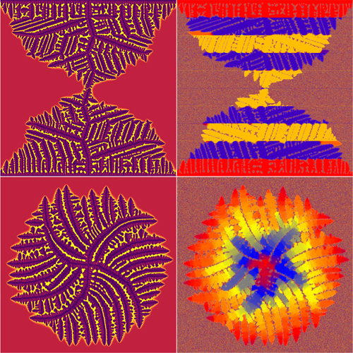
Figure 3: This new phase field model can also be used to predict methods to control microstructural patterns. The patterns on the left indicate concentration of solute, while the patterns on the right indicate the orientation of the crystal. The structures on the top were induced by laying down horizontal lines of fixed orientation. This causes the main stalk to zigzag. In the lower figures, we include orientation pinning centers that spin at a fixed rotation rate, causing the dendrite to develop a pinwheel structure.
For More Information on this Topic
J. Warren (Metallurgy Division, NIST); Jack Douglas (Polymers Division, NIST); R. Kobayashi (Hokkaido University, Japan); L. Granasy (RISSPO, Hungary); W.C. Carter (MIT)
Back to Top
Advanced Metallizations for Sub-100 nm Electronics
Electrodeposited copper is rapidly replacing aluminum for on-chip “wiring” because of its lower electrical resistivity, superior electromigration behavior, and the ability to fill fine features without the formation of seams or voids. As feature dimensions go below 100 nm, difficulties in maintaining performance are anticipated. We are addressing these issues through a combination of modeling and experimental efforts. In FY2003, we have pushed the quantitative limits of the Curvature Enhanced Accelerator Coverage (CEAC) mechanism developed in the Metallurgy Division of NIST. Exploration of the mechanism has yielded new electrochemical processing routes for improved metallization and is guiding the development of advanced metallizations beyond copper as well as new processing routes such as ruthenium barriers for seedless electrodeposition of copper.
NIST Contact: Thomas P. Moffat and Daniel Josell
This project is meeting the microelectronics industry’s need for improved device metallizations by exploring advanced materials and process models for superconformal film growth. In FY2003 we have:
• Developed a two-step process for obtaining superfill during silver electrodeposition;
• Demonstrated superconformal feature filling using ruthenium barriers without copper seeds;
• Described an exact solution for feature filling under conditions of fixed total catalyst coverage;
• Extended the CEAC mechanism to explain surface stabilization of planar deposits during deposition of metals in electrolytes containing surfactant additives;
• Quantified consumption of adsorbed catalyst (neglected in previous CEAC models) which can substantially affect feature filling under certain deposition conditions.
Filling of trenches and vias with silver and copper is quantitatively explained by the Curvature Enhanced Accelerator Coverage Mechanism (CEAC) developed at NIST. Our current measurement and modeling effort is focused on copper and silver metallizations, the latter metal having the lowest resistivity of any element and, thus, having potential on-chip applications.
A two-step process for superfill of high aspect ratio features during silver deposition was demonstrated for the first time. In this process, the catalyst is adsorbed on the patterned wafer prior to metal deposition; in traditional copper processing, a single electrolyte contains both the catalyst and the metal ions. As explained by the CEAC mechanism, this process offers the possibility of improved filling of finer features with higher aspect ratios through minimization of the conformal “incubation” period of growth. In addition, the plating bath requires fewer components and is thus easier to maintain under industrial conditions.
In a review of NIST research by International Sematech in November 2000, Aaron Frank, Program Manager for Copper Deposition, requested that we also examine a growing problem for on-chip interconnects: poor deposition of seed layers as features shrink. In response to this request, we demonstrated in FY 2003 that superconformal electrodeposition directly on ruthenium barrier layers on patterned substrates eliminates the difficulties associated with sputter-depositing copper seeds on tantalum and titanium nitride barriers, again allowing filling of finer features with higher aspect ratios (See Figure 1).
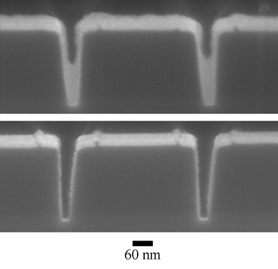
Figure 1: Bottom-up copper fill during electrodeposition in 50 nm wide trenches with no copper seed is visible in the top image. The patterned dielectric with the ruthenium barrier alone is visible in the bottom image.
Computer codes, that quantitatively predict superconformal deposition in fine features through the CEAC mechanism, evaluate concentration fields in the electrolyte as well as surface coverage of adsorbed catalyst on a moving boundary. Our closed-form solution for fixed initial coverage of catalyst can be used to assess the accuracy of these codes, increasing the reliability of their predictions when applied to more complex conditions including catalyst accumulation and consumption.
In a development with application far beyond the microelectronics industry, our recent publication on the CEAC mechanism of brightening is the first to quantitatively explain the impact of adsorbed catalyst on surface stabilization during growth. This work is possibly the most significant advance in understanding surface stabilization since the growth of surface perturbations due to concentration gradients was first described. It is as significant to creating shiny electrodeposits of metal on a car bumper as it is to reducing defect-inducing surface roughness in feature filling for microelectronics.
Figure 2: The geometry used to define the exact solution for the superconformal filling of a trench. The metal deposits at the bottom corners of the trench have met in the middle where a new, even more rapidly moving, growth front emanates.
Electrochemical and surface analytical measurements on planar substrates were used in FY2003 to establish rates of catalyst consumption that affect both feature filling and, quite likely, the microstructure of the metal deposits. Previous CEAC-based models have discounted such consumption, and this work demonstrates the reasonableness of such assumptions for the previously studied conditions. It also extends the understanding of CEAC mechanism operation to the less than ideal deposition conditions for which catalyst consumption is significant.
Selected Project Publications for FY2003
D. Josell, T.P. Moffat, and D. Wheeler. “An Exact, Algebraic Solution for the Incubation Period of Superfill,” J. Electrochem. Soc., (in press).
D. Josell, D. Wheeler, C. Witt, and T.P. Moffat. “Seedless Superfill: Copper Electrodeposition in Trenches with Ruthenium Barriers.” Electrical and Solid-State Letters, (in press).
G.B. McFadden, S.R. Coriell, T.P. Moffat, D. Josell, D. Wheeler, W. Schwarzacher, and J. Mallett. “ A Mechanism for Brightening: Linear Stability Analysis of the Curvature Enhanced Accelerator Coverage Model.” J. Electrochem. Soc., (in press).
D. Josell, S. Kim, D. Wheeler, T.P. Moffat, and S.G. Pyo. “Interconnect Fabrication by Superconformal Iodine-Catalyzed Chemical Vapor Deposition of Copper.” J. Electrochem. Soc., 150 (5), C368–C373 (2003).
D. Wheeler, D. Josell, and T.P. Moffat. “Modeling Superconformal Electrodeposition Using the Level Set Method.” J. Electrochem. Soc., 150 (5), C302–C310 (2003).
B.C. Baker, C. Witt, D. Wheeler, D. Josell, and T.P. Moffat. “Superconformal Silver Deposition Using KSeCN Derivitized Substrates.” Electrochemical and Solid-State Letters, 6 (5), C67–C69 (2003).
T.P. Moffat, B. Baker, D. Wheeler, and D. Josell. “Accelerator Aging Effects During Copper Electrodeposition.” Electrochemical and Solid-State Letters, 6 (4), C59–C62 (2003).
S.G. Pyo, S. Kim, D. Wheeler, T.P. Moffat, and D. Josell. “Seam-Free Fabrication of Sub-Micrometer Copper Interconnects by Iodine-Catalyzed Chemical Vapor Deposition.” J. Appl. Phys., 93 (2), 1257–1261 (2003).
B.C. Baker, M. Freeman, B. Melnick, D. Wheeler, D. Josell, and T.P. Moffat. “Superconformal Electrodeposition of Silver from a KAg(CN)2-KCN-KSeCN Electrolyte.” J. Electrochem. Soc., 150 (2),C61–C66 (2003).
T.P. Moffat, D. Wheeler, C. Witt, and D. Josell. “Superconformal Electrodeposition Using Derivitized Substrates.” Electrochemical and Solid-State Letters, 5 (12), C110–C112 (2002).
D. Josell, B. Baker, C. Witt, D. Wheeler, and T.P. Moffat. “Via Filling by Electrodeposition: Superconformal Silver and Copper and Conformal Nickel.” J. Electrochem. Soc., 149 (12), C637–C641 (2002).
Our findings have also been conveyed to the U.S. microelectronics industry, academia, and other national laboratories through more than 15 external presentations in the last year, including an invited presentation at Intel’s Portland, Oregon facility. Project publications generated 100+ citations in the past year.
For More Information on this Topic
D. Josell, D. Wheeler, T.P. Moffat (Metallurgy Division, NIST)
Back to Top
High Throughput Data Analysis of Multicomponent Multiphase Diffusion Data
Multicomponent diffusion processes are part of many complex industrial processes. Reliable data and analysis are critical to effective understanding and development of such processes and the resulting materials. For example, control of multicomponent diffusion is essential for optimizing heat treatments, predicting service life times, and determining optimal material properties. Developing and modeling these processes requires efficient methods to use and store massive amounts of diffusion data as well as improved techniques for understanding multicomponent diffusion data.
NIST Contact: Carelyn E. Campbell and William J. Boettinger
An improved understanding of multicomponent multiphase diffusion is motivated by two major industrial interactions: the DARPA/General Electric (GE)-led AIM (Advanced Insertion of Materials) program, which highlighted the need for modeling multicomponent diffusion in Ni-base superalloys, and the March 2002 NIST roadmapping workshop on “Databases for Computational Thermodynamics and Diffusion Modeling.” As a part of the AIM program, a diffusion mobility database for Ni-base superalloys was developed. An essential resource in developing the diffusion mobility database was the NIST Diffusion Data Center, which catalogs all of the diffusion work between 1950 and 1980. The developed diffusion mobility database was then used in conjunction with the NIST-developed thermodynamic database for Ni-base superalloys to simulate various multicomponent diffusion couples. The diffusion simulations were compared to experimental results provided by GE. Figure 1 shows one such comparison for a Ni/Rene88 diffusion couple. The experimental and calculated composition profiles are in good agreement, but several questions remain on how to best analyze the data from multicomponent diffusion couple experiments. Current diffusion simulation methods predict the diffusion coefficients as function of composition and time; however, the ability to extract comparable experimental diffusion coefficients from multicomponent diffusion couples is limited.
The second industrial interaction motivating further diffusion work was the result of interactions at the March 2002 NIST workshop on “Databases for Computational Thermodynamics and Diffusion Modeling.” One of the action items from the 2002 workshop was the development of a diffusion work group to address a variety of multicomponent diffusion questions as well as to promote the development of multicomponent diffusion mobility data.
Based on the needs identified in 2002, a diffusion workshop series began at NIST founded on the following objectives:
• To improve communication among experts in multicomponent diffusion measurement, analysis, and simulation.
• To establish the most efficient method for extracting diffusion data (diffusion coefficients, fluxes, marker location) from multicomponent diffusion couple experiments.
• To provide a forum to solve common diffusion software execution problems.
• To agree on a common diffusion mobility database assessment procedure.
• To establish a general approach to data handling and diffusion modeling in ordered phases.
• To develop standard problems and a website for inter-laboratory comparison of diffusion simulation methods and data extraction techniques.
Following the above objectives, the first of a series of workshops on “The High Throughput Analysis of Multicomponent Multiphase Diffusion Data” was held at NIST, March 27–28, 2003. The workshop format was designed to encourage active discussion among participants and hands-on computer demonstrations.
Presentations on available software for simulating multicomponent diffusion couples included discussions of the DICTRA (Diffusion Controlled Transformation) finite-difference diffusion code and Profiler. The MultiDiflux software code was presented as a tool for determining interdiffusion coefficients from multicomponent data. The development of diffusion mobility databases was presented.
Discussions also included a review of diffusion notation, the advantages and disadvantages of various inverse methods (methods used to determine diffusion coefficients from experimental composition profiles), and a review of various experimental techniques. The group also assessed the limitations of various commonly used methods, including the limits of the Darken approach and the Boltzmann–Matano method.
Representatives from industry presented experiences in using various diffusion software codes as well as experimental methods. A strong industrial need was articulated for developing the understanding of diffusion in amorphous material, specifically in bulk metallic glasses, and for developing multicomponent diffusion data and modeling in ordered phases.
In the first diffusion workshop, several action items were identified, including the development of a website to post the group's progress and of various tools for teaching multicomponent diffusion. A second diffusion workshop in the fall of 2003 will highlight an introduction to first principle calculations for diffusion, experimental issues in obtaining quality data, and an analysis of multicomponent diffusion in multiphase materials. The complexity associated with multicomponent multiphase diffusion is shown in Figure 2 comparing the experimental and calculated Co composition profiles for the Rene88/IN100 diffusion couple. At 1150 ºC, IN100 is a two-phase mixture of γ and γ´. While the diffusion simulations consider the two-phase equilibrium during the diffusion simulations, experimental methods for extracting diffusion coefficients from multiphase materials are not well defined.
At both the 2002 NIST Workshop and the 2003 Diffusion Workshop, both industrial and academic diffusion experts described the value of having the NIST Diffusion Data Center converted to a searchable electronic form. The Diffusion Data Center represents a unique collection of diffusion work up until 1980, which is cataloged by author, diffusion system, and selected keywords. The collection contains translations of published works and difficult-to-obtain government reports and theses. To preserve this work and to make it more widely available, the Metallurgy Division is converting the paper-based catalog to a searchable electronic format. Once the catalog is converted to an electronic format, it will be made available on the NIST website. The work will then focus on converting the difficult-to-find papers, reports, and theses to an electronic format, which can be accessible via the NIST website.
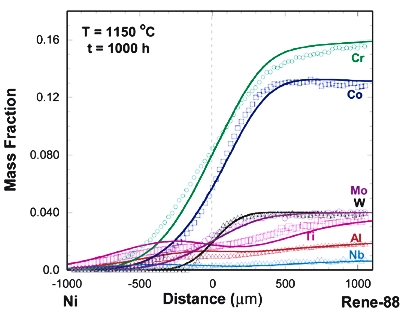
Figure 1: Calculated (solid lines) and experimental (symbols) composition profiles for the Ni/Rene88 diffusion couple at 1150 ºC for 1000 h. Experimental profiles from GE-CRD.
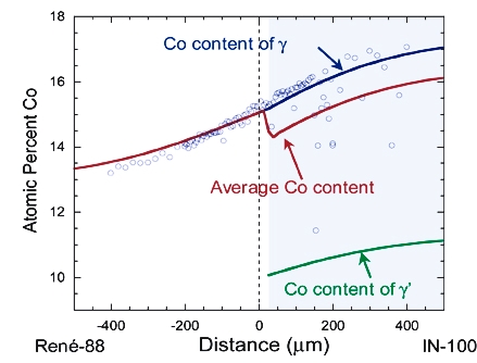
Figure 2: Calculated and measured (symbols) Co composition profiles in the Rene88/ IN100 diffusion couple at 1150 ºC for 1000 h. At 1150 ºC, IN100 is a two phase mixture of γ + γ´. The red line is the calculated average Co profile. The blue line is the Co profile in the γ phase and green is the Co profile in the γ´ phase. The light blue region indicates the predicted two-phase region in the couple after 1000 h at 1150 ºC. Experimental data from GE-CRD.
Through the continuing NIST Workshops, action plans for the Diffusion Working Group, and development and application of multicomponent diffusion mobility databases, NIST interaction with academia and industry will continue to better address critical diffusion issues. Ultimately, this increased accessibility to diffusion data will provide material producer and user industries with a variety of tools to more efficiently use and model multicomponent diffusion as a vital part of process modeling.
For More Information on this Topic
C.E. Campbell, W.J. Boettinger, U.R. Kattner (Metallurgy Division, NIST); J.-C. Zhao (GE-CRD)
C.E. Campbell, W.J. Boettinger, and U.R. Kattner. “The Development of a diffusion mobility database for Ni-base superalloys.” Acta Mater, 50, 775–792 (2002).
www.ctcms.nist.gov/~cecamp/workshop.html
Back to Top
Modeling Dynamics, Damping and Defects for Perpendicular Magnetic Recording Media
In its accelerating march toward ever higher recording densities, the hard disk drive industry is moving toward perpendicular recording, where the magnetization of the written bits is directed perpendicular to the disk surface. One of the metrology needs generated by the shift to perpendicular recording is the characterization of inhomogeneity in the media. This article describes our development of models that enable measurement of inhomogeneity in perpendicular media by ferromagnetic resonance.
NIST Contact: Robert D. McMichael
One of the growing metrology needs of the hard drive industry is the ability to characterize the new generation of perpendicular recording media, where the information is stored as magnetic bits magnetized perpendicular to the disk surface. To store these bits, it is desirable to have media with small, nearly decoupled grains with strong, uniform anisotropy and easy axes directed along the disk normal. Typical grain sizes in the new media are approximately 10 nm.
Characterization of the average properties of perpendicular media is routinely accomplished by magnetometry. However, there is a significant need for information about the inhomogeneity of perpendicular media, particularly the angular easy axis distribution and the distribution of anisotropy fields. Inhomogeneity of the media impacts the bit writing process, analysis of bit stability, and media noise in the read process.
Information about the dispersion of the crystallographic axes can be obtained from x-ray diffraction, but magnetic coupling may force two crystallographically distinct grains to behave as a single magnetic grain, so a purely magnetic measurement of the dispersion angle would be more closely related to the performance of the media.
For variations in the anisotropy field, the only estimates currently available are based on TEM compositional analysis coupled with anisotropy studies on bulk materials. Here again, a direct, purely magnetic measurement would give a clearer indication of the magnetic performance of the media.
The new perpendicular media, with aligned anisotropy axes, is much better suited to ferromagnetic resonance measurements than longitudinal media. Ferromagnetic resonance is a peak in the transverse susceptibility at a frequency that corresponds to precession of the magnetization about its equilibrium orientation. The width of the ferromagnetic resonance peak, or “line width,” is the combined effect of damping and inhomogeneity. While there are well-established models for damping, better models of inhomogeneity were needed for interpretation of line width data.
Through our modeling the dynamics of inhomogeneous films, we have laid the theoretical support needed for interpretation of line width data to obtain inhomogeneity information on magnetic thin films.
Previously, there were two known models of ferromagnetic resonance line broadening by inhomogeneity: the “local resonance” model and the “two-magnon” model. The local resonance model assumes that interactions are not important, and the line width is therefore a direct measure of the inhomogeneity strength. The “two-magnon” model includes interactions but, because it is a result of perturbation theory, is limited to weak inhomogeneity. The two-magnon linewidth depends quadratically on the inhomogeneity strength. The models give very different results, but both models have been successfully used to describe separate sets of linewidth data.
Figure 1: In the absence of interactions, inhomogeneity leads to local resonances at a distribution of frequencies, leading to a broadened resonance line. Interactions cause narrowing of the envelope peak described by the two-magnon model.
To understand the relationship between the local resonance and two-magnon models of line width, we modeled a series of inhomogeneous films with different grain sizes and different levels of inhomogeneity, and we computed the eigenmodes of the magnetization motion (Figure 1). We found that the behavior of the magnetization dynamics depends on the relative strengths of the interactions and the inhomogeneity. For a uniform film, the eigenmodes are spinwaves (“magnons” in quantum mechanics), and inhomogeneities or strong interactions cause mixing of the spin wave modes in agreement with the two magnon model. For strong inhomogeneities relative to interactions, the dynamics were localized on individual grains in agreement with the local resonance model. These results are summarized in Figure 2, where small grain sizes correspond to strong intergranular interactions, and large grains correspond to weak interactions. These results unify the local resonance and two-magnon models.
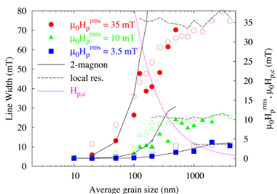
Figure 2: Line widths as a function of grain size in a Permalloy film calculated by eigenmode analysis for three random field strengths Hp. (Open and closed symbols are for two methods of computing line width from the eigenmode spectrum.) The linewidth transitions smoothly from the local resonance model for large grains (weak interactions) to the two-magnon model when grains are small. The pink line indicates where interactions and inhomogeneity are roughly equal.
The full eigenmode analysis takes a significant amount of computation time, making it a poorly suited technique for data fitting. However, the results in Figure 2 suggest a simple first approximation; for a given combination of microstructure and inhomogeneity, the lesser of the two-magnon model and the local resonance model is likely to be valid, except in the range where they are similar.
Figures 3 and 4 show two-magnon and local resonance line width calculations for perpendicular media with thickness 15 nm and grain size 10 nm with an average anisotropy field of 1.4 T (14 kOe). In these figures, the top diagram portrays the local resonance result, the green curve is the two-magnon model with dipolar interactions only, and the blue and pink curves are for fractional and full exchange coupling. For the given inhomogeneity strengths, the two magnon model results are expected to be a good approximation to the line width, but for larger values of inhomogeneity, the two magnon results will exceed the local resonance values and the local resonance results would be valid.
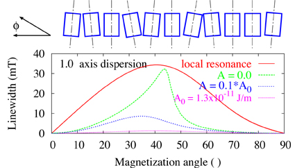
Figure 3: Local resonance and two-magnon line widths resulting from tilting of the easy axis directions in perpendicular recording media with 10 nm grains. Two magnon results are calculated for three values of exchange coupling.
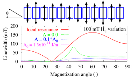
Figure 4: Local resonance and two-magnon line widths resulting from anisotropy variations in perpendicular recording media with 10 nm grains. Two magnon results are calculated for three values of exchange coupling.
These results show that the ferromagnetic resonance line width can be a sensitive probe of inhomogeneity in perpendicular recording media with the ability to differentiate damping, c-axis dispersion, and anisotropy variations. For weak inhomogeneity, the two-magnon model becomes valid, and the linewidth can also provide information about exchange coupling.
A ferromagnetic resonance apparatus with the frequency and field ranges necessary to measure perpendicular media is in the design phase.
For More Information on this Topic
R.D. McMichael, W.F. Egelhoff, Jr. (Metallurgy Division, NIST) R.D. McMichael, D.J. Twisselmann, and A. Kunz. Phys. Rev. Lett., 90, Art. No. 227601 (2003).
Back to Top
Artifacts in Ballistic Magnetoresistance Measurements
Magnetic sensors play a central role in many important technologies ranging from data storage to health care to homeland security. A common need among these technologies is higher sensitivity and smaller size. Advances in the past year in the Ballistic Magnetoresistance (BMR) effect appeared to provide enormous progress in sensitivity in nanoscale devices. The scientific press reported it as one of the major discoveries of the year. Unfortunately, it appears to be wrong. Experiments at NIST have found that several simple artifacts can account for the results. NIST is taking a leading role in designing artifact-free metrology to provide reliable data to the magnetic sensor industry.
NIST Contact: William F. Egelhoff, Jr.
Magnetic sensors play a central role in many important technologies. To name just a few, computer hard disk drives use magnetic sensors to read stored data (Figure 1), magnetoencelophalography uses magnetic sensors to image brain wave activity, and bio-hazard detectors use magnetic sensors to detect magnetic beads bio-tagged for anthrax, botulism, cholera, and other pathogens.
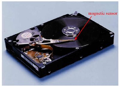
Figure 1: Computer hard disk drives use a magnetic sensor to read data.
A common need among these technologies is higher sensitivity and smaller size. With higher sensitivity and smaller size, more data could be stored on a hard disk, higher resolution imaging of brain activity would be possible, and earlier warnings of bio-contamination could be given.
Currently, the Giant Magnetoresistance (GMR) effect is used for the best small-scale sensors. A GMR sensor can, at best, exhibit a ≈ 15 % change in electrical resistance in response to a magnetic field. Shock waves went through the magnetic-sensor community in 2003 when a value for the Ballistic Magnetoresistance effect (BMR) of 100,000 % was published and a value of 1,000,000 % was reported at a major scientific conference.
Understanding these results suddenly became a high priority for the magnetic-sensor community. For example, Seagate, the world’s leading hard-disk drive manufacturer, sent Dr. Erik Svedberg, a physicist in its research labs, to work with us half-time in 2003 to investigate BMR. Seagate selected to work with NIST because we already had a strong program in place to investigate BMR and a network of collaborators that included those groups reporting the high BMR values. NIST had initiated the BMR research program prior to these reports because earlier less-sensational reports of BMR looked promising but faced a number of problems. BMR samples had poor reproducibility, poor stability, and poor reliability. The fabrication techniques were poorly understood, and there was no theory to explain the magnitude of the BMR effect. It was felt that NIST might help with what is often a long, hard road from a laboratory demonstration of a concept to a commercially successful device.
As the NIST program developed over the past two years, it became clear that other labs were able to achieve much higher BMR values, some in the 100 % to 700 % range, while NIST results rarely exceeded 10 %. The trend accelerated in 2002 as these other labs began reporting results of 3,000 % to 10,000 %. These BMR values were reported as major discoveries in Science, Science News, and Physics News.
In late 2002 and early 2003, scientists from these other labs visited NIST to demonstrate how they achieved these results. NIST staff analyzed the experiments and found them to be subject to a variety of artifacts that can mimic BMR. The small BMR values that NIST had measured were directly attributable to more careful experimental design that excluded the artifacts.
The most common artifact is a result of magnetostriction, in which the length of a magnetic wire changes length in a magnetic field. Figure 2 illustrates the geometry that produced some of the sensational effects attributed to BMR. Two Ni wires are brought together with a gap of ≈ 20 µm. The gap is bridged by electrodepositing Ni in a way that forms a nanocontact with one of the Ni wires. This nanocontact is thought to have dimensions on the order of 10 nm. When a magnetic field is applied along the axis of one of the wires, a sharp increase in the electrical resistance of the nanocontact is observed, as illustrated in the inset in Figure 2. The results were interpreted as BMR assuming that the magnetic field was magnetizing the two sides of the nanocontact in opposite directions and the resulting magnetic domain wall impeded the flow of electrons, thereby increasing the measured resistance.
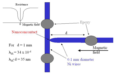
Figure 2: An illustration of the geometry used to generate sensational apparent BMR values.
A simpler explanation accounts for the result: the magnetic field also makes the Ni wire shorter. Using the magnetostriction constant λ for Ni and the length of free wire, the calculated shortening is 35 nm. This distance is enough to stretch and severely deform a 10 nm nanocontact, increasing its electrical resistance. In fact, in experiments at NIST using electrochemical techniques, it was possible to break and reform nanocontacts thus giving what would correspond to infinite BMR.
Further experiments at NIST using alloy wires whose composition is tailored to have a magnetostriction constant of zero showed no resistance change in a magnetic field. These wires were magnetic and should exhibit BMR if the effect was as claimed, casting further doubt on the high values reported.
Another approach investigated at NIST involved replacing the Ni wires with Ni thin films deposited on wafers. The strength of bonding between the Ni and the wafer anchored the Ni films and suppressed the shortening effect. In this geometry, the nanocontact showed no resistance change, further supporting the conclusion that the high BMR values were not true BMR.
When informed about the NIST results, one of the other labs responded with a method to produce the high BMR values in magnetic nanocontacts electrodeposited at an unusually large voltage on wafers. NIST examined the techniques and found that the unusually large deposition voltage did not produce a solid contact. Instead, the deposit consisted of loosely assembled magnetic particles. When a magnetic field was applied, a compaction of the powder could be observed in a microscope. The small magnetic particles, upon becoming magnetized in the same direction, were clumping together under the magnetostatic attraction, as illustrated in Figure 3.
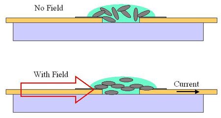
Figure 3: An illustration of how magnetostatic forces cause magnetic particles to clump together to create conducting paths.
In samples made this way, the no-field case was the high resistance state, and the with-field case was the low resistance state. When the particles clumped together, they created additional current-carrying paths to lower the electrical resistance. There was no evidence of anything resembling true BMR in these samples.
A preliminary report of these artifacts was presented at the March Meeting of the American Physical Society in 2003. A more comprehensive report of the work will be presented at the Magnetism & Magnetic Materials Conference in January 2004.
Experiments are continuing at NIST to put BMR on a firm scientific foundation. Although a conclusive answer is not available at this point, the results, so far, suggest that there may be a small BMR effect but not one that is large enough to be of great interest to the magnetic-sensor community. NIST’s work on this topic is likely to be completed early in FY04.
“The technical challenges facing the data storage industry in the next 10 years are so broad and so deep that the industry cannot do it alone. We need researchers like you here at NIST to help us.”
Dr. Sining Mao
Senior Manager, Recording Heads Division, Seagate Technology
For More Information on this Topic
E. Svedberg (Seagate); N. Garcia (CSIC, Madrid); H. Chopra (SUNY-Buffalo); R. McMichael, T. Moffat, J. Mallett (Metallurgy Division, NIST); M. Stiles (Electron and Optical Physics Division, NIST); C. Powell (Surface and Microanalysis Science Division, NIST)
Back to Top
Phase Field Modeling of the Electrochemical Interface
Many important problems in electrochemistry, such as void formation during plating in vias and trenches for on-chip metallization or dendrite formation during recharging of batteries, involve complex topologies that are not easily treated by existing models. The phase field modeling technique has had considerable success studying similar interfaces, with much of the fundamental work performed by researchers in the NIST Metallurgy Division, but the work has almost exclusively focused on solidification. This project seeks to bridge the gap between the traditional electrochemical and phase transformation modeling communities.
NIST Contact: Jon E. Guyer and William J. Boettinger
Electrodeposition is increasingly being applied to sub-micrometer features with convoluted morphologies, such as the “copper damascene” process of the micro-electronics industry. In this size regime, factors become important which have been safely neglected in macroscopic models of electrochemistry. For example, as length scales shrink, surface curvature becomes an important consideration; subtle interactions between surface energy and the selective adsorption of different species on the electrode surface can no longer be ignored. Furthermore, traditional models of electrochemical interfaces, such as that of Gouy–Chapman–Stern, take the interface between phases (the transition between electrode and electrolyte) to be abrupt. Such treatments have difficulty tracking a real electrochemical interface, which is often convoluted or can have changing topology, because the boundary conditions on that interface depend on its position, which is part of the unknown solution.
The phase field technique is an alternative approach to modeling phase transformations that has had considerable success in the past decade in the modeling of solidification. The method employs a thermodynamic variable, which is a function of position and time, to describe whether the material is solid or liquid. The behavior of this variable is governed by a partial differential equation that is coupled to the relevant transport equations for the material. The interface between the phases is described by smooth but highly localized changes of this variable. It is not necessary to explicitly track the interface between phases or to apply any boundary conditions there. The method is computationally demanding, but it is powerful because changes in complex interfaces and topology occur naturally.
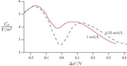
Figure 1: Differential capacitance calculated by our model.
Motivated by the successful phase field models of solidifying interfaces, we seek to expand NIST’s “phase field toolkit” into electrochemistry. As a first step to applying the method to convoluted electrochemical interfaces, we have developed a 1D model by making a limited set of assumptions: mass and volume constraints, Poisson’s equation, ideal solution thermodynamics in the bulk phases, and a simple description of the competing energies in the electrode/electrolyte interface.
Equilibrium Interface
The interface between two phases containing free charges is known to develop a charged “double layer.” For instance, a layer of excess electrons at the surface of a metal will mirror a layer of excess cations in the adjacent electrolyte. Despite the simple assumptions made in its formulation, our model spontaneously produces just such a double layer. Even though both the total charge and the charge in each bulk phase are zero, we find that there is some non-zero charge distribution in the interface, just as in physical systems. Both electrochemical theory and experiments on inert systems show that the surface charge is directly coupled to the surface energy and that both depend on the potential across the interface. In particular, at the “point of zero charge” (PZC), where the surface charge is zero, the surface energy has a maximum. Independent calculations of surface energy and surface charge using our model exhibit exactly the relationship expected from traditional theories.
The “differential capacitance” is defined by the change in surface charge with potential. The value predicted by classical models of the electrochemical interface depends on the hyperbolic cosine of potential near the PZC and becomes a constant for larger potential differences. The differential capacitance calculated by our model, however, exhibits complex shapes with multiple extrema, as seen in Figure 1. This behavior bears a much stronger resemblance to experimental measurements, such as in Figure 2, than to previous theories.
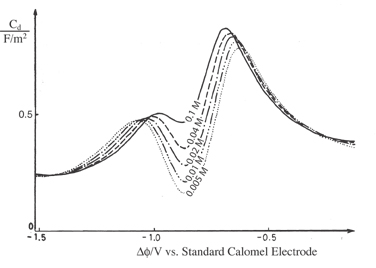
Figure 2: Experimental measurements of differential capacitance on Ag(100) electrodes in aqueous solutions of NaF. [Reprinted from J. Electroanal. Chem. 138, G. Valette (1982) 37–54), with permission from Elsevier.]
Turning now to the examination of electrodeposition and electrodissolution, when the overpotential (the deviation from the equilibrium potential difference across the interface) is not zero, current will flow and the interface will move. The classical description for the relationship between current and overpotential is the empirical Butler–Volmer relation (Figure 3).
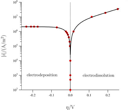
Figure 3: Current vs. overpotential calculated by our model (symbols) and predicted by classical Butler–Volmer equation (line).
In contrast, phase field models typically assume that the rate of change of the phase field is directly proportional to some driving force. Despite making such a simple assumption about the kinetic behavior, the rich interplay among composition, charge, electrostatic potential, and thermodynamic stability gives rise to current-overpotential behavior that agrees very well with the predictions of traditional electrochemistry (Figure 3).
At large overpotentials, we find that the most electroactive cation becomes depleted at the interface nearly to zero. The concentration gradient can be no steeper, limiting the rate of cation diffusion to the interface. In order to carry more current than this diffusion-limited value, the charge structure of the interface shifts to allow deposition of less electroactive species. Figure 4 shows two different times after the current has been changed from 0.005% to 500% of the limiting current for the deposition of M, leading to alloy deposition of M and N.
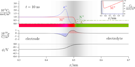
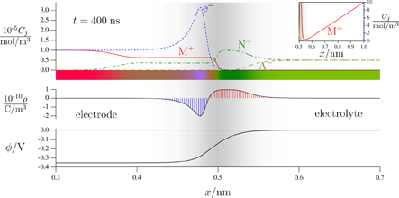
Figure 4: Profiles of the ion concentrations, charge density, and electrostatic potential at two different times after the current was changed from 102 A/m2 to 107 A/m2. The gray band indicates the position of the diffuse phase field interface.
By correctly describing the fundamental physics, our model spontaneously produces differential capacitance curves strongly reminiscent of experiments, nonlinear current-overpotential behavior, and alloy deposition, all without making ad hoc assumptions. Future work will focus on further relating the parameters of the phase field model with those of traditional electrochemistry, examining larger physical domains, and to extending the model to two dimensions.
For More Information on this Topic
J. Guyer, W. Boettinger, J. Warren (Metallurgy Division, NIST); G. McFadden (Mathematical and Computational Sciences Division, NIST)
Back to Top
NEMI–NIST–TMS Workshop on Tin Whiskers: Cause and Effect
This NEMI–NIST–TMS workshop brought together key researchers to compare in detail research that has been done in the area of tin whiskers, and to see if a consensus could be developed on a basic model defining the conditions for whisker formation, or, if not, on the work required to reach such a consensus. The end goal is to provide direction to the electronics industry in developing deposition processes that will assure that long-lifecycle products will not experience catastrophic failure due to whisker growth.
NIST Contact: William J. Boettinger and Maureen Williams
Since the mid 1940s, the phenomenon of metallic growths from electrodeposited surface finishes on electronic components has been observed and studied. Electrodeposited surface finishes applied to the component leadframe protect the material from corrosion and improve solderability of the components prior to board assembly. These metallic growths are referred to as whiskers and may form different shapes, as seen in Figure 1.
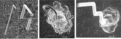
Figure 1: Three different whisker types from bright Sn coatings; a) Filament with tip and base shown in insert; b) Odd shaped eruption with filimenery growths; c) filament growing from an eruption.
The most commonly used commercial surface finishes are Tin (Sn) based. Sn whiskers (filament type whiskers are typically 1 µm diameter and several mm long) can grow from the Sn plate and cause electrical shorts and failures. Tin–lead (Pb) alloys have been used extensively for surface finishing of electronic components because Pb was found to be effective in retarding Sn whisker growth and keeping production costs low. Since Pb-free solder alloys have been introduced, electronic manufacturers are seeking a new surface finish technology that will prevent Sn whisker growth without the use of Pb. Whiskers are generally believed to grow to relieve residual stress in electroplated Sn. Figure 2 shows a schematic of compressive stresses in electrodeposited Sn plating resulting in the growth of a Sn whisker. Some of the key factors that have been found to influence Sn whisker growth are: deposit thickness, diffusion, thermal stresses, substrate material, electrolyte type, plating conditions, temperature, humidity, organic and inorganic inclusions, grain size and shape, and interdiffusion barriers. In spite of this wealth of information, a basic understanding of whisker growth and its prevention does not currently exist.
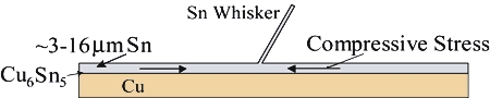
Figure 2: Schematic of Sn whisker growth from a Sn electrodeposited plating.
The National Institute of Standards and Technology (NIST), the National Electronics Manufacturing Initiative (NEMI), and The Minerals, Metals & Materials Society (TMS) co-sponsored a one-day workshop, “Tin Whiskers: Cause and Effect,” on Sunday, March 2, at the San Diego Convention Center. The event was held in conjunction with the 2003 TMS Annual Conference and Exhibition.
The agenda consisted of four presentations during the morning and round table discussions in the afternoon. The 44 attendees represented a variety of industrial, academic, and government organizations, including Analog Devices, Brocade Communications Systems, Cookson Electronics, Hanyang University, HP, IBM, Intel, KAIST, Kyocera, Los Alamos National Lab, Michigan State, Millenium Chemicals, Motorola, Oak Ridge National Lab, Research in Motion, Sandia National Laboratory, Shipley TI, Sun Yat-Sen University (Taiwan), SUNY at Buffalo, Technic, The Aerospace Corporation, University of Kentucky, and Washington State University. All of the participants contributed to a lively afternoon discussion of the papers presented and current theories.
Stress in Electroplated Sn
Dr. Chen Xu of Cookson Electronics outlined his work on understanding the whisker growth rate and carrying out structural and chemical characterizations of whisker growths. He presented a “whisker index” — a proposal to characterize whiskers and presented data on this factor as a function of various types of Sn plating. He discussed the use of x-ray diffraction (XRD) for measuring stress in Sn plated films, showing the changes in stress as a function of time. His data shows that compressive stress in the film leads to whisker growth, while tensile stress does not.
He presented data to show that a nickel (Ni) under layer will result in tensile stress in the Sn layer, and he saw no whisker growth when a Ni layer was deposited between the Cu and Sn layers.
Spontaneous Growth of Tin Whiskers
Dr. Dong Nyung Lee of the School of Materials Science and Engineering, Seoul National University showed results of microstructure characterization using SEM techniques, including angle of growth, and pole figures. To release the compressive stress in the tin film, tin whiskers grow from the grain whose surface oxide is sheared. The whisker growth is controlled by the expansion of prismatic dislocation loop on the slip plane by climb, that is, by means of the operation of the Bardeen–Herring dislocation source. Whisker growth continues until the stress is relieved.
Tin-Whisker Microstructural Analysis
Dr. George T. Galyon of the IBM Server Group provided a critical analysis of the literature outlined in his Annotated Sn Whisker Bibliography, noting that there appear to be necessary conditions for whisker formation (i.e., stress) that are not always sufficient to explain the overall phenomena. He provided a great deal of information on the use of the Focused Ion Beam (FIB) tool in examining whiskers. Very little, and only recent, work has been reported using this new tool, and it seems to provide considerable additional insight into whisker structures. His observations indicate that whisker growth is the result of a recrystallization of the tin at the base of the whisker resulting in additional material pushing the whisker out of the film.
Focused Ion Beam, Transmission Electron Microscopy, and Synchrotron Radiation
Dr. King N. Tu, of the Department of Materials Science and Engineering at UCLA, performed studies on tin whiskers with focused ion beam (FIB) imaging, cross-section transmission electron microscopy (XTEM) observation, and synchrotron radiation (SR) micro-diffraction analysis. Morphology of whiskers and orientation relationship between a whisker and grains in the tin plating has been studied by FIB and XTEM. A large amount of precipitates in the grain boundaries were observed. The precipitation of Cu6Sn5 intermetallic is believed to maintain the driving force for spontaneous whisker growth.
Discussion Summary
Discussions established that Sn whiskers are caused by compressive stress in the Sn plated film, and that material somehow moves through the grain boundaries to form a whisker. Whiskers grow from material deposited at the base of the whisker. The formation of Cu6Sn5 intermetallics in the Sn grain boundaries may contribute to the growth of a compressive stress. The whisker may take advantage of weakness in the oxide film to erupt.
While no specific mechanism for Sn whisker growth was established, several questions were posed. Some of these questions included:
• Why is recrystallization of Sn necessary for whisker growth?
• What is the mechanism by which the Sn is transported to the whisker base?
Discussions also determined several areas that require further study to determine the growth mechanism:
• The role of Pb in suppressing whisker formation; the role of a surface oxide layer;
• The role of texture;
• The role of impurities; and
• The role of a diffusion barrier.
An understanding of the details of the nucleation process is also needed. The most important conclusion was that further systematic experimental work must be done to establish the growth mechanism.
Currently at NIST, efforts are focused on analyzing the average stress relaxation in electrodeposited films as function of time. These experiments concentrate on in situ stress measurements during the plating process and post-plating. Additional experimental work is planned in collaboration with NEMI members.
“I consider your [NIST Metallurgy Division] group a key asset to industry in making these decisions on the soundest possible scientific basis. There is no comparable body of expertise anywhere in the world that matches that found in your group.”
Dr. George T. Galyon
(IBM) — Chairman, NEMI Tin Whisker Modeling Committee
For More Information on this Topic
W.J. Boettinger, M. Williams (Metallurgy Division, NIST); R. Gedney (NEMI); K.-W. Moon (University of Maryland)
Back to Top
Kolsky Bar: Materials Properties at High Strain Rates and High Heating Rates
Materials processed in industry are frequently placed simultaneously under applied high strain and heating rates. Understanding, predicting, and simulating these processes require databases for materials properties and constitutive equations verified under similar conditions. NIST has responded to these industrial needs by developing a unique testing facility for measuring the needed data and validating the appropriate material models under controlled, high rates of straining and heating.
NIST Contact: Richard Fields and Debasis Basak
Machining processes such as turning, milling, drilling, broaching, etc., are the most commonly used methods of producing precision metal parts. Efficient machining requires a thorough knowledge of the machine/tool/workpiece interactions. This includes understanding material behavior under the conditions of machining. Furthermore, competition has pushed industry to machine parts as rapidly as possible. This has led to the development of codes that predict machining behavior and guide the development of the most efficient machining practices. These codes require, as input, mechanical property data that is not commonly available for most alloys of commercial interest.
At the tool/workpiece interface, the material being removed is subject to extremely high forces and temperatures. The high temperatures arise from the work dissipated by the large and rapid straining. They also result from the friction between the tool and the workpiece material. It has been estimated that the straining occurs at a rate between 103 s–1 and 106 s–1, while the heating takes place at rates up to 106 K/s. The rapid heating is important because most microstructural features cannot change to their equilibrium structure in such a short time. Previous attempts at collecting high temperature data elsewhere have relied on low rates of heating and thus measured the properties of inappropriate microstructures. It is the controlled, high heating rate that makes the current facility unique.
The facility is built around a conventional Kolsky Bar (sometimes called a Split Hopkinson Pressure Bar) shown in Figure 1. An air gun fires a striker bar at speeds up to 50 m/s at the incident bar. On impact, the striker bar generates a roughly square elastic wave in the incident bar twice the length of the striker bar and traveling at nearly 5000 m/s. This wave propagates down the incident bar to the sample and compresses the sample between the incident bar and the transmitted bar. The elastic strain at any time introduced into the transmitted bar during this process is proportional to the stress in the sample at that time and the elastic strain reflected back into the incident bar is proportional to the strain rate experienced by the sample at that time. By analyzing the strain signal records, the stress/strain behavior of the sample material can be determined under controlled high strain rates.
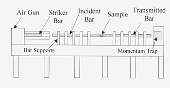
Figure 1a: Schematic diagram of Kolsky Bar apparatus.
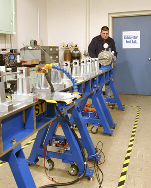
Figure 1b: Photograph of NIST’s Kolsky Bar facility.
A millisecond-resolution pulse heating facility, which relies on rapid resistive “Joule heating” of the specimen by the passage of an electric current pulse of sub-second duration, is used to heat the specimen. The connections for the current input can be seen in Figure 2. Two high-speed pyrometers are used simultaneously during the test. A spot pyrometer measures the specimen temperature with microsecond-resolution, and an imaging pyrometer records the temperature distribution in the specimen during the test. The output from the spot pyrometer is also used to control the specimen temperature. When the desired temperature is reached, the electric current to the specimen is either automatically turned off or a feedback control program is activated to achieve isothermal conditions in the specimen, prior to impact.
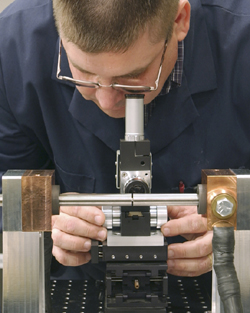
Figure 2: The current for heating is introduced through copper blocks and graphite bearings to the incident and transmitted bars, and then through the sample seen in the middle. The sample temperature is monitored by the pyrometer being focused on it.
This facility was developed to provide insight and data for high speed machining of commercial alloys. To date, it has been used mainly for copper, 303 stainless steel, AISI 1045 steel, and 7075 aluminum alloy. The results of this research are described under “High Speed Machining” elsewhere in this annual report. The data are being provided to industry and other alloys of commercial interest are being investigated.
More than a dozen papers and talks have been presented on this topic in the three years that this project has been underway. Additional papers are being drafted.
Since the facility was developed, other applications for it have arisen. The World Trade Center Twin Tower collapses were initiated by the impact of two commercial airliners. NIST has undertaken the modeling of these impacts to more fully understand the events leading up to the failure of the towers. The models require high strain-rate mechanical properties. The Kolsky Bar facility is providing the rate dependence of plastic deformation for the many types of structural steel in the buildings.
Another application concerns the behavior of projectiles such as those used as military tank penetrators. It has been found that the Kolsky Bar test is one of the best predictors of thermal localization of deformation and the self-sharpening behavior desired in penetrator materials. The Kolsky Bar facility is providing a project in the Metallurgy Division that is investigating new penetrator materials with a rapid assessment of whether their materials or processing routes are improving penetration behavior.
Lastly, considering the significant number of conventional Kolsky bars in use in the U.S., an effort has been initiated to compare the consistency of measurements made with these instruments. To date, NIST has compared its results on 1045 steel and copper with similar results at Aberdeen Proving Grounds and Los Alamos National Laboratory. Such intercomparisons will help improve and maintain consistency of dynamic materials properties measurements.
New applications for this unique facility are being pursued in the areas of dynamic fracture and crack arrest of high strength pipeline steels, bullets and body armor for the Office of Law Enforcement Standards, and additional issues in manufacturing. Since certain types of explosions involve intense, rapid, radiative heating followed by a shock wave, it is felt that the new Kolsky Bar facility may play an important role in research relating to homeland security.
For More Information on this Topic
Richard Fields, L. Levine, R. deWit (Metallurgy Division, NIST); R. Rhorer, R. Polvani, K. Jurrens, R. Ivester, H. Soons, M. Kennedy, B. Dutterer, (Manufacturing Metrology Division, NIST); T. Burns (Mathematical and Computational Sciences Division, NIST); H. Yoon (Optical Technology Division, NIST); Debasis Basak (University of Tennessee); M. Davies (University of North Carolina, Charlotte)
Back to Top
|